Flexible winding and inductor integrated with capacitor characteristic and manufacturing method of flexible winding
A production method and technology of capacitance characteristics, applied in the direction of inductors with magnetic cores, inductors, transformers/inductor coils/windings/connections, etc., can solve problems such as adverse effects of EMI filtering performance, reduce volume and improve filtering efficiency effect
- Summary
- Abstract
- Description
- Claims
- Application Information
AI Technical Summary
Problems solved by technology
Method used
Image
Examples
Embodiment 1
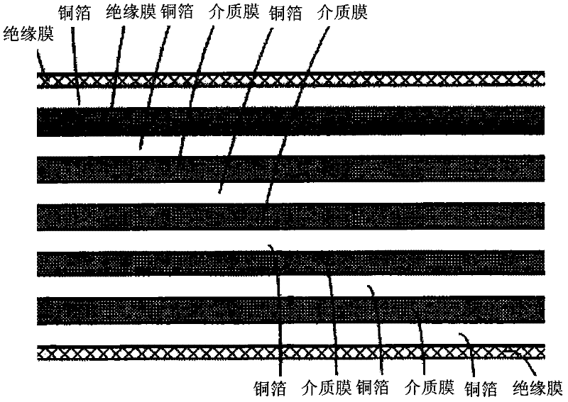
[0035] image 3 A schematic structural diagram of a flexible winding integrated with capacitive properties provided for an embodiment of the present invention, as shown in image 3 As shown, the flexible winding includes: a dielectric film 1, a first metal layer 2 and a second metal layer 3 with instantaneous self-recovery properties. Wherein, the first metal layer 2 and the second metal layer 3 are arranged on both sides of the dielectric film 1 respectively. The structure of the two layers of metal with an insulating layer in between constitutes a thin film capacitor structure of the flexible winding, wherein the first The metal layer 2 and the second metal layer 3 serve as electrodes of the thin film capacitor structure respectively.
[0036] An embodiment of the present invention provides a flexible winding integrated with capacitive characteristics, the flexible winding includes a dielectric film and a first metal layer on both sides of the dielectric film and a second m...
Embodiment 2
[0063] Figure 17 It is a flowchart of a manufacturing method of a flexible winding provided by an embodiment of the present invention, and the flexible winding described here is the flexible winding provided in the above-mentioned embodiment. Such as Figure 17 As shown, the method includes:
[0064] Step 1701: setting a first metal layer on one side of the dielectric film, and vapor-depositing a second metal layer with instantaneous self-recovery properties on the other side of the dielectric film;
[0065] It should be noted that, if the first metal layer can be a copper layer and conductive copper paste is used, the copper layer on the surface of the dielectric film can specifically be: coating the non-metallized surface of the dielectric film by printing or the like In this way, the conductive copper paste is coated on the dielectric film; the conductive copper paste is cured by heating to form a copper layer. It can be seen that the use of conductive copper paste to m...
PUM
| Property | Measurement | Unit |
|---|---|---|
| capacitance | aaaaa | aaaaa |
Abstract
Description
Claims
Application Information


