Semiconductor device and producing method thereof

A manufacturing method and semiconductor technology, applied in the fields of semiconductor/solid-state device manufacturing, semiconductor devices, semiconductor/solid-state device components, etc., can solve problems such as difficulty in reducing the form factor of PoP packaging, and limited pins for adapter board packaging.

Active Publication Date: 2011-08-31
TAIWAN SEMICON MFG CO LTD
View PDF4 Cites 35 Cited by
  • Summary
  • Abstract
  • Description
  • Claims
  • Application Information

AI Technical Summary

Problems solved by technology

However, PoP packaging is difficult to reduce the form factor
Additionally, pack

Method used


Image

  • Semiconductor device and producing method thereof
  • Semiconductor device and producing method thereof
  • Semiconductor device and producing method thereof

Examples


Embodiment Construction

[0048] The manufacture and use of the embodiments of the present invention are described below. It should be readily appreciated, however, that the embodiments of the invention provide many suitable inventive concepts that can be implemented in a wide variety of specific contexts. The specific embodiments disclosed are only used to illustrate the making and use of the present invention in specific ways, and are not intended to limit the scope of the present invention.

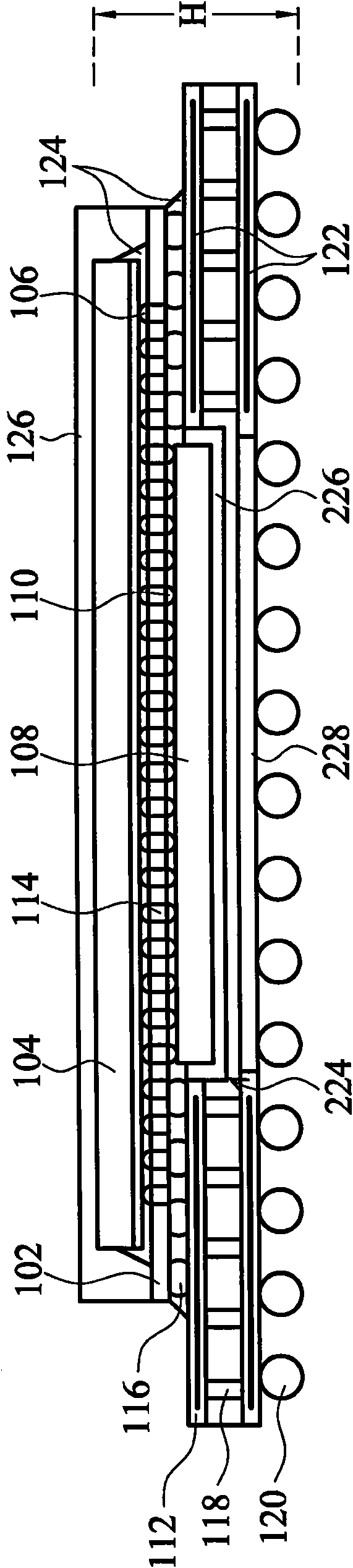
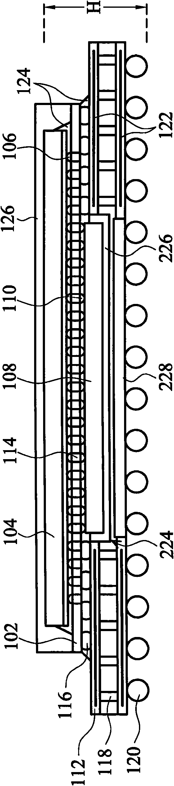
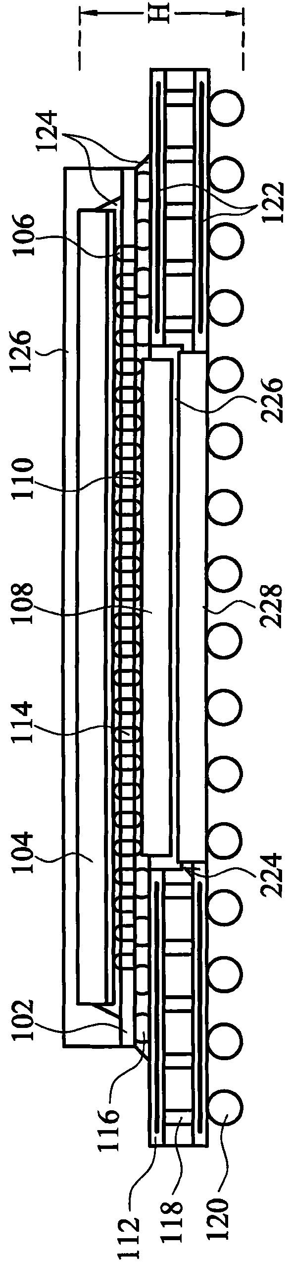
[0049] Please refer to Figure 1a , which shows an interposer 102 having a first integrated circuit chip 104 attached to a first side of the interposer 102 by a first set of conductive bumps 106 and by a second set of conductive bumps according to an embodiment 110 and attached to the second integrated circuit chip 108 on the second side of the interposer 102 . The first set of conductive bumps 106 and the second set of conductive bumps 110 may include microbumps with a diameter ranging from about 5 to 50 mic...


PUM


Abstract

The invention discloses a three-dimensional semiconductor packaging using an interposer. The invention provides a semiconductor device and a producing method thereof. The semiconductor device comprises a first chip whose first side is electrically coupled to the interposer and a second chip whose second side is electrically coupled to the interposer. The interposer is electrically coupled to a below substrate, such as a packaging substrate, a high-density interconnector, a printed circuit board and so on. The substrate is provided with a recess, making a second chip being disposed in the recess. The recess allows using quite a small conductive bump, thereby quite a large amount of conductive bumps can be used. A radiating fin can be placed in the recess to assist the second chip to dissipate heat.

Description

technical field [0001] The present invention relates to a semiconductor device and a manufacturing method thereof, in particular to a three-dimensional semiconductor package using an interposer. Background technique [0002] Since the invention of the integrated circuit, the semiconductor industry has continued to grow rapidly due to continuous improvements in the integration density of various electronic components (ie, transistors, diodes, resistors, capacitors, etc.). Mainly, the improvement of integration level comes from the continuous shrinking of the minimum feature size, which allows more components to be integrated into the existing chip area. [0003] These improvements in integration are essentially two-dimensional (2D), since the volume occupied by the integrated components is actually located on the surface of the semiconductor wafer. Although advances in lithography technology have brought considerable benefits to the fabrication of 2D integrated circuits, the...

Claims


Application Information

Patent Timeline
IPC IPC(8): H01L25/00H01L25/065H01L23/13H01L23/00H01L21/50
CPCH01L24/97H01L2924/01322H01L2924/15311H01L2224/97H01L2224/16225H01L2224/73204H01L2224/32225H01L2224/73253H01L2924/14H01L2924/00012H01L2224/81H01L2924/00
Inventor 郑心圃陈锦棠侯上勇史朝文谢政杰余振华
Owner TAIWAN SEMICON MFG CO LTD
Why Eureka
Try Eureka