Method for processing blind buried hole on multilayer circuit board

A technology of multi-layer circuit boards and blind and buried vias, which is applied to the formation of electrical connection of printed components, etc., can solve the problems of extremely high control and electroplating requirements, less than 80% yield rate of finished products, and difficult wiring, so as to overcome the phenomenon of board warping. , The effect of improving product quality and reducing production costs

Active Publication Date: 2012-10-10
BOMIN ELECTRONICS CO LTD +1
View PDF0 Cites 2 Cited by
  • Summary
  • Abstract
  • Description
  • Claims
  • Application Information

AI Technical Summary

Problems solved by technology

[0006] The above case 1 requires mechanical blind drilling technology, which requires extremely high blind hole depth control and electroplating, and the finished product yield rate is less than 80%. Cases 2 and 3 require at least two asymmetric laminations. The finished products produced by this process 100% of the board is warped, and the yield rate of the finished product is about 80%. Electroplating, copper thickness is thick, it is difficult to make lines of 0.1 / 0.1mm and below

Method used


Image

  • Method for processing blind buried hole on multilayer circuit board
  • Method for processing blind buried hole on multilayer circuit board
  • Method for processing blind buried hole on multilayer circuit board

Examples


Embodiment 1

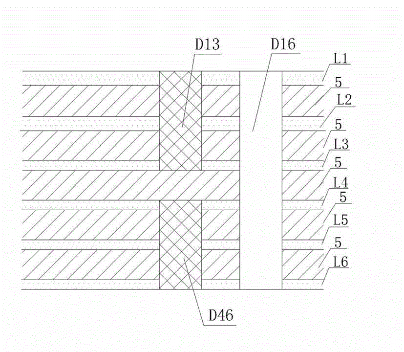
[0027] Such as Figure 4 As shown, the layers of a 4-layer circuit board are: top layer L1, second layer L2, third layer L3, and bottom layer L4. There is a dielectric layer 5 between each layer, and the thickness of the dielectric layer 5 is 0.08mm. Open a 0.25mm mechanical buried hole la in the second layer L2 and the third layer L3, then use a resin plug to bury the hole 1a, and then grind the plate surface with residual resin, electroplate again, make the core board layer circuit, and press it as a whole, and finally in the top layer L1 Open 0.15mm laser blind hole 1b, open 0.15mm laser blind hole 1b on the bottom layer L4, the top layer L1 laser blind hole 1b is electroplated with the mechanical buried hole la of the second layer L2 to form a pad connection, and the bottom layer L4 laser blind hole 1b is connected to the third The mechanical buried hole la of layer L3 is electroplated to form pad connection, and the last four-layer circuit board is drilled through hole 1c...

Embodiment 2

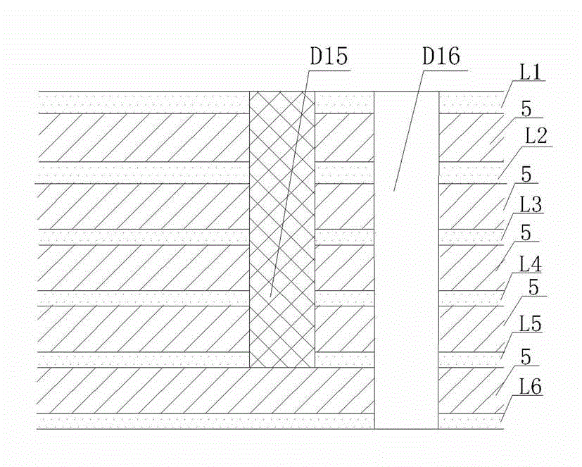
[0029] Such as Figure 5 As shown, the layers of a 6-layer circuit board are: top layer L1, second layer L2, third layer L3, fourth layer L4, fifth layer L5, bottom layer L6, with a dielectric layer 5 between each layer, The thickness of the dielectric layer 5 is 0.08 mm, and a 0.25 mm mechanical buried hole 1a is opened in the second layer L2 to the fifth layer L5, and then the hole 1a is buried with a resin plug, and then the remaining resin is ground on the flat surface, and the core layer is made by electroplating again The circuit is pressed together as a whole, and finally a 0.15mm laser blind hole 1b is opened on the top layer L1. The laser blind hole 1b of the top layer L1 is electroplated with the mechanical buried hole la of the second layer L2 to form a pad connection, and finally the six-layer circuit board is drilled as a whole. 1c.

Embodiment 3

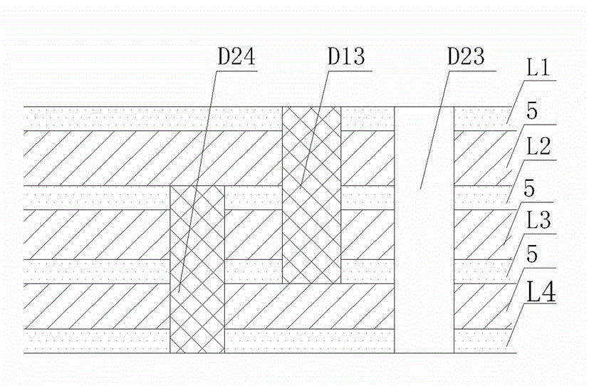
[0031] Such as Figure 6 As shown, the layers of a 6-layer circuit board are: top layer L1, second layer L2, third layer L3, fourth layer L4, fifth layer L5, bottom layer L6, with a dielectric layer 5 between each layer, The thickness of the interlayer dielectric layer 5 is 0.08mm. Laser buried holes la are drilled from the second layer L2 to the third layer L3, and laser blind holes la are drilled from the fourth layer L4 to the fifth layer L5. The aperture size of the laser blind holes is 0.1mm , and then use the electroplating filling process to fill the laser blind hole la, then grind the copper particles and burrs protruding from the flat surface, make the core layer circuit, and press it as a whole. Finally, open a 0.15mm laser blind hole 1b on the top layer L1, and open the bottom layer L6 0.15mm laser blind hole 1b, the top layer L1 laser blind hole 1b and the laser buried hole la of the second layer L2 are filled and electroplated to form a pad connection, and the bot...


PUM


Abstract

The invention relates to a method for processing a blind buried hole on a multilayer circuit board, which belongs to the technical field of laser drilling. The technical key point of the invention comprises the following steps of: (1) confirming a position needing hole opening of the traditional mechanical blind buried hole circuit board; (2) processing a buried hole on an inner-layer plate of the position needing hole opening and electroplating again after filling resin into the buried hole for grinding to form a butting joint pad; and (3) drilling a laser blind hole on an upper-layer circuit board at at least one side of the processing buried hole and butting the laser blind hole with the pad formed electroplating on the mechanical buried hole to form a blind buried hole. Compared with the prior art, the invention has the advantages of shortening the process flow, thoroughly overcoming the phenomenon of board bending generated by asymmetric laminating structure design due to asymmetric hole layer distribution, solving the problem that a copper layer is relatively thicker and is adverse to the manufacture of a thin circuit because the traditional mechanical blind buried hole process outer layer is electroplated for many times, reducing the pressing frequency of board layers and the manufacture difficulty and improving the product quality.

Description

technical field [0001] The invention relates to a method for processing blind buried holes on a multilayer circuit board, in particular to a method for using laser drilling on a mechanical blind buried hole design circuit board, which belongs to the technical field of laser drilling. Background technique [0002] With the continuous maturity and promotion of laser drilling technology, the traditional mechanical blind buried hole board gradually faded out of the historical stage, but there are still some special-purpose boards still using the traditional mechanical blind buried hole design. The printed circuit board using the traditional mechanical blind buried hole technology has a long process, and the lamination is mostly asymmetrical lamination, and the board is seriously warped. At the same time, because the outer layer has to undergo multiple platings, the copper thickness is not conducive to the production of thin lines. [0003] Example 1, a four-layer mechanical blin...

Claims


Application Information

Patent Timeline
Patent Type & Authority Patents(China)
IPC IPC(8): H05K3/40
Inventor 覃新邓宏喜韩志伟罗旭
Owner BOMIN ELECTRONICS CO LTD
Why Eureka
Try Eureka