Supercharge Your Innovation With Domain-Expert AI Agents!

Timing processing method and circuit for synchronous static random accessible memory (SRAM)

A processing method and timing technology, applied in the field of electronics, can solve the problems of increasing the running time of the timing path of the synchronous SRAM and reducing the working speed of the synchronous SRAM, so as to save the latching time and improve the working speed.

Active Publication Date: 2013-04-17
HUAWEI TECH CO LTD
View PDF3 Cites 0 Cited by
  • Summary
  • Abstract
  • Description
  • Claims
  • Application Information

AI Technical Summary

Problems solved by technology

Because the address latch will consume a certain amount of time to latch the address, this increases the timing path running time of the synchronous SRAM and reduces the working speed of the synchronous SRAM.

Method used


Image

  • Timing processing method and circuit for synchronous static random accessible memory (SRAM)
  • Timing processing method and circuit for synchronous static random accessible memory (SRAM)
  • Timing processing method and circuit for synchronous static random accessible memory (SRAM)

Examples


Embodiment Construction

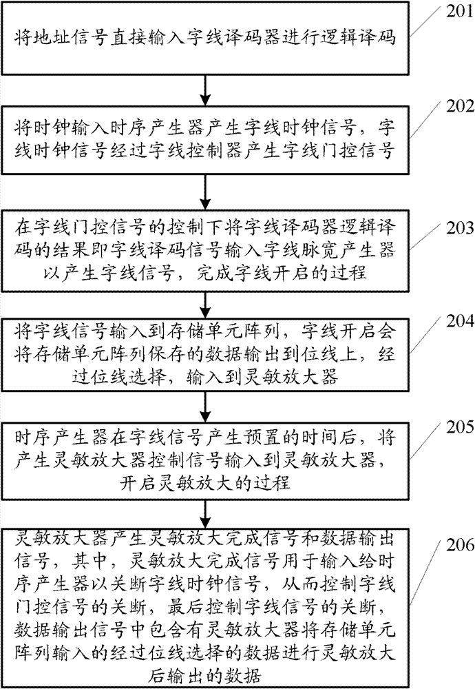
[0027] Embodiments of the present invention provide a timing sequence processing method and circuit of a synchronous SRAM, which can increase the working speed of the synchronous SRAM and enable the synchronous SRAM to work at a higher frequency.

[0028] In order to make the purpose, features and advantages of the present invention more obvious and understandable, the technical solutions in the embodiments of the present invention will be clearly and completely described below in conjunction with the accompanying drawings in the embodiments of the present invention. Obviously, the following The described embodiments are only some, not all, embodiments of the present invention. All other embodiments obtained by those skilled in the art based on the embodiments of the present invention belong to the protection scope of the present invention.

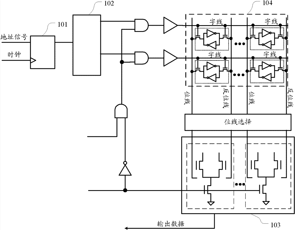
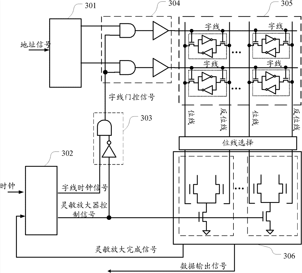
[0029] A schematic diagram of timing processing of a synchronous SRAM provided by an embodiment of the present invention, as shown in ...


PUM


Abstract

A timing processing method and circuit for synchronous Static Random Accessible Memory (SRAM) is disclosed. The method comprises: inputting address signals to a word line decoder directly to perform logic decoding; generating each signal by means of settings in timing for each device, and performing sensitivity amplification on data inputted from a memory cell array and selected by bit lines and outputting the data afterwards, i.e. generating a data output signal. The synchronous SRAM circuit comprises a word line decoder, a timing generator, a word line controller, a word line pulse width generator, a memory cell array and a sense amplifier.

Description

technical field [0001] The invention relates to the field of electronic technology, in particular to a timing processing method and circuit of a synchronous SRAM. Background technique [0002] Static Random Accessible Memory (SRAM) is very helpful to improve system performance because it can save the data stored in it without refreshing the circuit. The first-level and second-level caches in the central processing unit (CPU, Central Processing Unit) use SRAM. In order to further improve the performance of the CPU, it is necessary to reduce the timing path of the CPU and integrate small-capacity external first-level or second-level caches. Level SRAM cache, and the timing path of SRAM is one of the critical timing paths, which limits the increase of the operating frequency of the CPU. SRAM can be divided into two categories from a high level: synchronous and asynchronous. Synchronous SRAMs use an input clock to initiate all data transactions (eg, read, write, deselect, etc....

Claims


Application Information

Patent Timeline
Patent Type & Authority Patents(China)
IPC IPC(8): G11C5/02G11C5/06
CPCG11C11/419G11C29/023G11C11/41G11C29/02G11C11/413G11C8/18G11C11/418
Inventor 季秉武周云明赵坦夫林崴
Owner HUAWEI TECH CO LTD
Features
  • R&D
  • Intellectual Property
  • Life Sciences
  • Materials
  • Tech Scout
  • Unparalleled Data Quality
  • Higher Quality Content
  • 60% Fewer Hallucinations
Learn More