Fan-out system in package (SIP) method

A system-level packaging and packaging layer technology, which is applied in the manufacture of electrical components, electrical solid-state devices, semiconductors/solid-state devices, etc., can solve problems such as unsuitable multi-layer packaging structures, and achieve the effect of high integration

Active Publication Date: 2011-09-07
NANTONG FUJITSU MICROELECTRONICS
View PDF3 Cites 26 Cited by
  • Summary
  • Abstract
  • Description
  • Claims
  • Application Information

AI Technical Summary

Problems solved by technology

In addition, the above method is not suitable for the manufacture of multi-layer packaging structures with complex wiring connections

Method used


Image

  • Fan-out system in package (SIP) method
  • Fan-out system in package (SIP) method
  • Fan-out system in package (SIP) method

Examples


Embodiment Construction

[0024] In the following description, numerous specific details are set forth in order to provide a thorough understanding of the present invention. However, the present invention can be implemented in many other ways different from those described here, and those skilled in the art can make similar extensions without violating the connotation of the present invention, so the present invention is not limited by the specific implementations disclosed below.

[0025] Secondly, the present invention is described in detail by means of schematic diagrams. When describing the embodiments of the present invention in detail, for convenience of explanation, the schematic diagrams are only examples, which should not limit the protection scope of the present invention.

[0026] The specific embodiments of the present invention will be described in detail below in conjunction with the accompanying drawings.

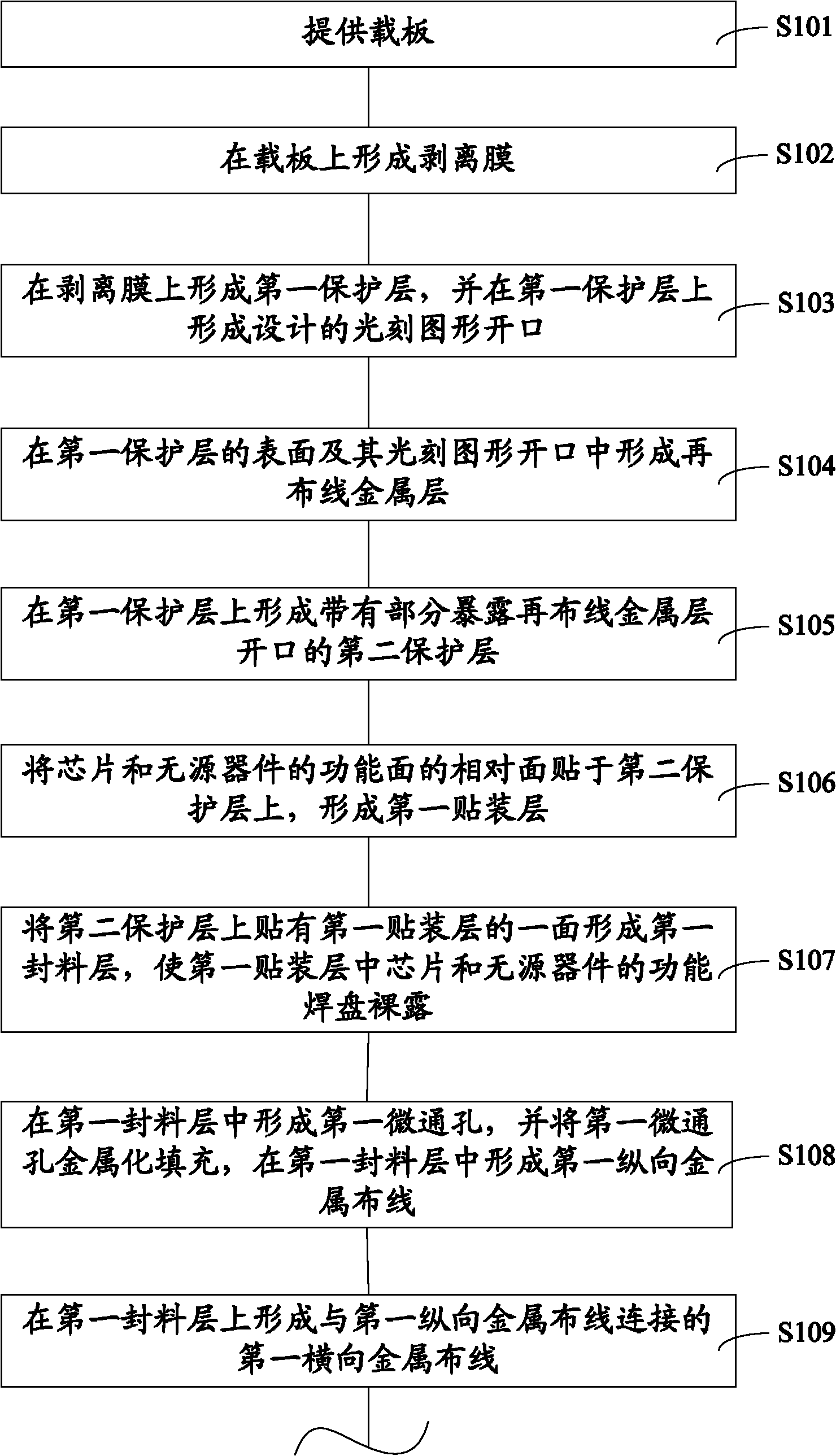
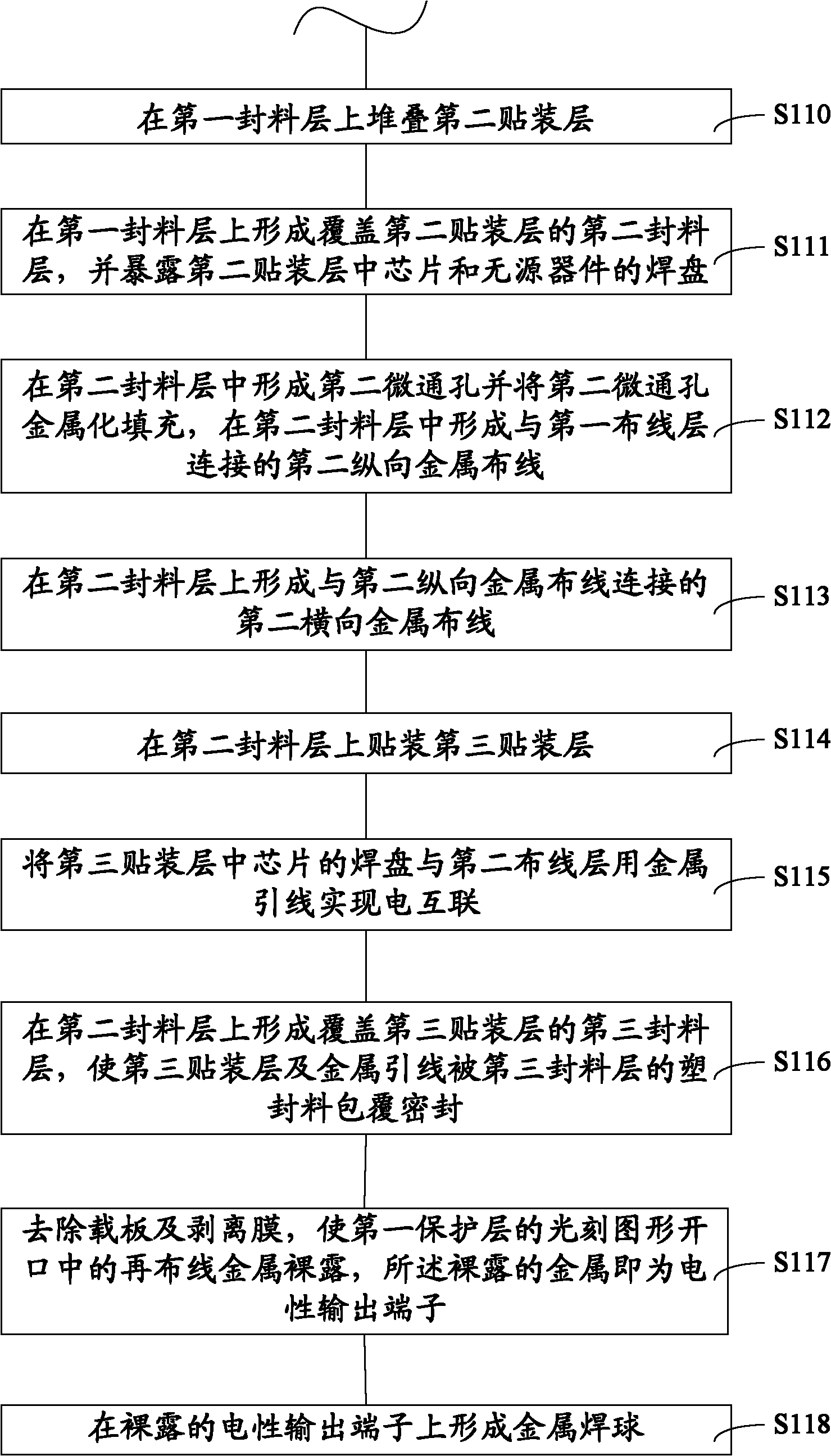
[0027] Such as figure 1 and figure 2 As shown, in one embodiment of the presen...


PUM


Abstract

The invention relates to a fan-out system in a package (SIP) method. The method comprises the following steps: providing a support plate; forming a stripped membrane on the support plate; forming protective layers on the stripped membrane and forming re-wiring metal layers in the protective layers; forming wiring packaging layers conducted with the re-wiring metal layers on the protective layers and forming wire bonding packaging layers on the wiring packaging layers; and removing the support plate and the stripped membrane to expose the re-wiring metal in the first protective layers and forming metal solder balls on the exposed re-wiring metal, wherein the packaging layers are electrically connected with each other. Compared with the prior art, the method which the invention requests to protect has the following beneficial effects: the final packaged products having the functions of the whole system instead of the functions of the single chip can be formed; the interference factors among the resistors, inductors and chips in the system are reduced; and besides, the more complex multilayer interconnection structure can be formed and higher integration level wafer SIP can be realized.

Description

technical field [0001] The invention relates to semiconductor technology, in particular to a fan-out system level packaging method. Background technique [0002] Wafer Level Packaging (WLP) technology is a technology that performs packaging and testing on the entire wafer and then cuts it to obtain a single finished chip. The size of the packaged chip is exactly the same as that of the bare chip. Wafer-level chip-scale packaging technology has completely subverted traditional packaging such as ceramic leadless chip carrier (Ceramic Leadless Chip Carrier) and organic leadless chip carrier (Organic Leadless Chip Carrier), etc. , small, short, thin and low-cost requirements. The size of the chip packaged by the wafer-level chip size packaging technology has reached a high degree of miniaturization, and the cost of the chip is significantly reduced with the reduction of the chip size and the increase of the wafer size. Wafer-level chip-scale packaging technology is a technolog...

Claims


Application Information

Patent Timeline
Patent Type & Authority Applications(China)
IPC IPC(8): H01L21/50H01L21/56H01L21/60
CPCH01L2224/48091H01L2924/10253H01L2224/48227H01L2924/30107
Inventor 陶玉娟石磊
Owner NANTONG FUJITSU MICROELECTRONICS
Why Eureka
Try Eureka