Vapor phase epitaxy device and vapor phase epitaxy method

A gas phase epitaxy and tail gas technology, applied in chemical instruments and methods, from chemically reactive gases, crystal growth, etc., can solve the problems of longer residence time, uneven center to edge, etc., to reduce flow instability, improve quality, the effect of reducing parasitic reactions

Active Publication Date: 2011-09-14
ZHEJIANG YUNFENG NEW ENERGY TECH
View PDF8 Cites 11 Cited by
  • Summary
  • Abstract
  • Description
  • Claims
  • Application Information

AI Technical Summary

Problems solved by technology

The main problem of this method is that as the points on the tray gradually move away from the center of rotation, the linear speed gradually increases, and the sector area of ​​the outer circle part is also much larger than that of the inner circle part, so that the wafers near the outer edge of the tray are larger than those n

Method used


Image

  • Vapor phase epitaxy device and vapor phase epitaxy method
  • Vapor phase epitaxy device and vapor phase epitaxy method
  • Vapor phase epitaxy device and vapor phase epitaxy method

Examples


Embodiment Construction

[0040] The core of the invention is to provide a vapor phase epitaxy device, which can effectively improve the uniformity of source gas and improve the product quality of semiconductor processing. Another core of the present invention is to provide a vapor phase epitaxy method using the above vapor phase epitaxy device.

[0041]In order to enable those skilled in the art to better understand the solution of the present invention, the present invention will be further described in detail below in conjunction with the accompanying drawings and specific embodiments.

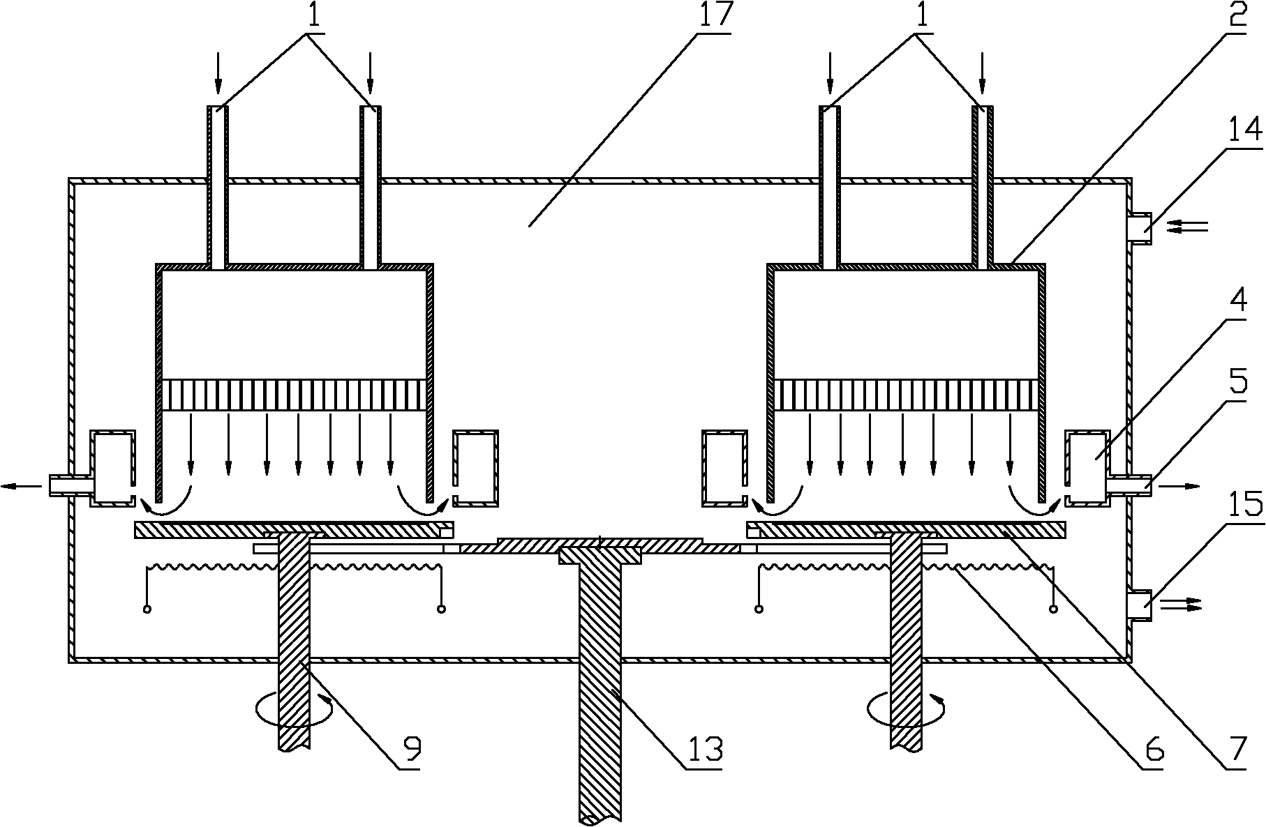
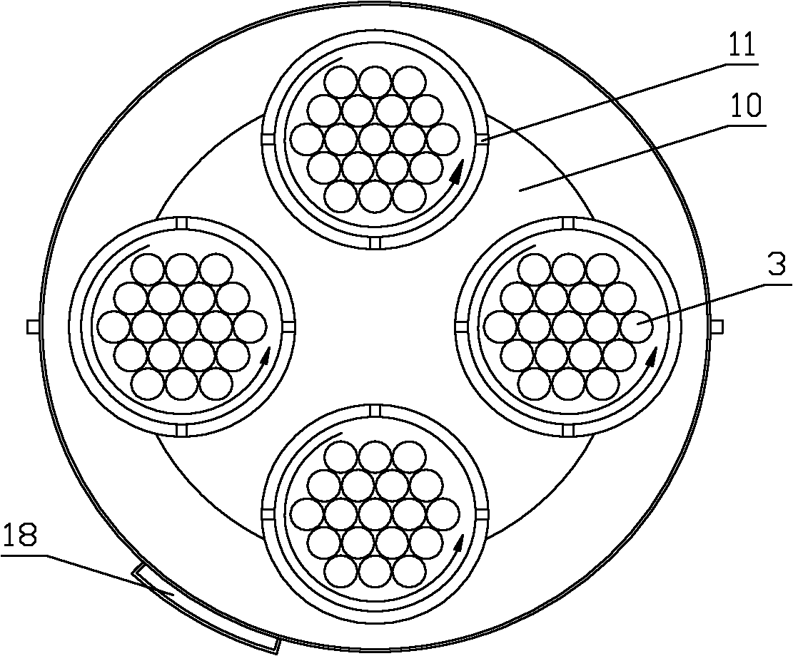
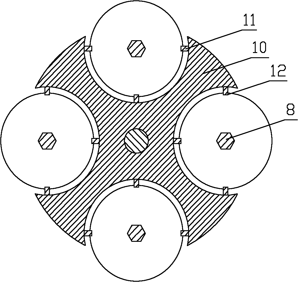
[0042] Please refer to Figure 1 to Figure 4 , figure 1 It is a structural schematic diagram of a specific embodiment of the vapor phase epitaxy device provided by the present invention; figure 2 It is a top view of a specific embodiment of the vapor phase epitaxy device provided by the present invention; image 3 for figure 2 Cross-sectional view of the vapor phase epitaxy setup shown; Figure 4 It is a conn...


PUM


Abstract

The invention discloses a vapor phase epitaxy device and a vapor phase epitaxy method. The disclosed vapor phase epitaxy device comprises a reaction chamber, a plurality of reaction gas spraying heads arranged in the reaction chamber, a plurality of trays corresponding to the plurality of reaction gas spraying heads, and a power shaft driving the trays, wherein the power shaft comprises revolution shafts and a plurality of rotation shafts, the rotation shafts correspond to the trays one by one; and the trays are respectively connected with the corresponding rotation shafts, or connected with the revolution shafts and the corresponding rotation shafts alternatively. By utilizing the vapor phase epitaxy device and the vapor phase epitaxy method, the flow instability in the chemical vapor phase epitaxy can be reduced effectively, the spurious response times can be decreased, also the problem of the thickness of a quantum well can be solved effectively, different selections can be provided for the growing process of different heterogenous junctions, and the quality of semiconductor elements can be improved.

Description

technical field [0001] The invention relates to the technical field of semiconductor production, in particular to a vapor phase epitaxy device and a vapor phase epitaxy method. Background technique [0002] Chemical vapor phase epitaxy (CVD or VPE) technology is widely used in the preparation of various semiconductor thin-film devices, including microelectronic chips, light-emitting diodes (LEDs), and solar photovoltaic cells. The basic process of chemical vapor phase epitaxy is that the source gas is introduced into the reactor from the gas source, and the gas particles reach the surface of the substrate through transport (convection and diffusion), and a chemical reaction occurs on the high-temperature substrate due to thermal excitation, so that on the wafer Deposit monocrystalline or polycrystalline thin films. [0003] In the preparation of chemical vapor phase epitaxy thin films, one of the main difficulties is how to achieve the uniformity of film thickness and compo...

Claims


Application Information

Patent Timeline
IPC IPC(8): C30B25/12C30B25/02
Inventor 左然徐永亮刘自强
Owner ZHEJIANG YUNFENG NEW ENERGY TECH
Why Eureka
Try Eureka