On-die termination circuit, memory device, memory module, and method of operating and training an on-die termination

A technology of memory modules and storage devices, used in static memory, digital memory information, information storage, etc.

Inactive Publication Date: 2011-09-21
SAMSUNG ELECTRONICS CO LTD
View PDF5 Cites 32 Cited by
  • Summary
  • Abstract
  • Description
  • Claims
  • Application Information

AI Technical Summary

Problems solved by technology

Other uses of ODT may require a delay circuit to turn on the ODT circuit after a predetermined delay from receipt of the ODT signal

Method used


Image

  • On-die termination circuit, memory device, memory module, and method of operating and training an on-die termination
  • On-die termination circuit, memory device, memory module, and method of operating and training an on-die termination
  • On-die termination circuit, memory device, memory module, and method of operating and training an on-die termination

Examples


Embodiment Construction

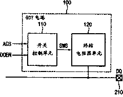
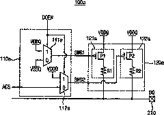
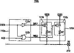
[0067] Various exemplary embodiments of the invention will be described more fully hereinafter with reference to the accompanying drawings that illustrate some exemplary embodiments of the invention. However, the inventive concepts may be embodied in many different forms and should not be construed as limited to the embodiments set forth herein. Rather, these exemplary embodiments are provided so that this disclosure will be thorough and complete, and will fully convey the scope of the inventive concept to those skilled in the art. In the drawings, the size and relative sizes of layers and regions may be exaggerated for clarity. Like numerals refer to like elements throughout.

[0068] It will be understood that, although the terms first, second, third etc. may be used herein to describe various elements, these elements should not be limited by these terms. These terms may be used only to distinguish one element from another. Thus, a first element discussed below could be t...


PUM


Abstract

A memory device comprises: a memory device having a memory core having a memory cell array; a data input / output pin connected to the memory core through a data buffer; and an on-die termination (ODT) circuit, comprising: a termination circuit configured to provide a termination impedance at the input / output data pin, the termination circuit having a switching device that selectively connects a termination impedance to the input / output data pin based on the presence of an asynchronous control signal (ACS), wherein the ACS is generated based on the presence of a memory WRITE command. The memory device may further comprise a training circuit comprising: an asynchronous signal delay configured to delay the signal path of the ACS signal to the termination circuit; and a comparing unit configured to compare a phase difference between the ACS signal and a reference signal, the comparing unit comprising a phase detector and a replica delay, wherein the replica delay is configured to delay the signal path of the ACS signal to the phase detector, and the phase detector is configured to output the phase difference as training result.

Description

[0001] priority [0002] This application claims priority to Application No. 2010-0016167 filed with the Korean Intellectual Property Office on Feb. 23, 2010, the contents of which are incorporated herein by reference. technical field [0003] Exemplary embodiments relate to on-chip terminators, and more particularly, to on-chip termination circuits, data output buffers, memory devices, memory modules, methods of operating the on-chip termination circuits, methods of operating the data output buffers, and training on-chip termination device method. Background technique [0004] An on-die terminator (ODT) is a signal termination circuit or element for impedance matching of signal lines located within a semiconductor chip. When signals are transmitted between devices via interface signal lines, signal reflection can be suppressed if the lines are impedance-matched. Signals connected between the memory controller and the memory device can be terminated, for example, using ODT...

Claims


Application Information

Patent Timeline
Patent Type & Authority Applications(China)
IPC IPC(8): G11C11/413
CPCG06F13/00G11C7/109G11C7/10G11C7/222G11C7/1057G11C7/1084G11C7/22
Inventor 全英珍
Owner SAMSUNG ELECTRONICS CO LTD
Why Eureka
Try Eureka