[0031] In order to further explain the technical means and effects of the present invention to achieve the intended purpose of the invention, the specific implementation, structure, features and effects of the electronic device proposed in accordance with the present invention will be described in detail below with reference to the drawings and embodiments Rear.
[0032] [First set of embodiments]
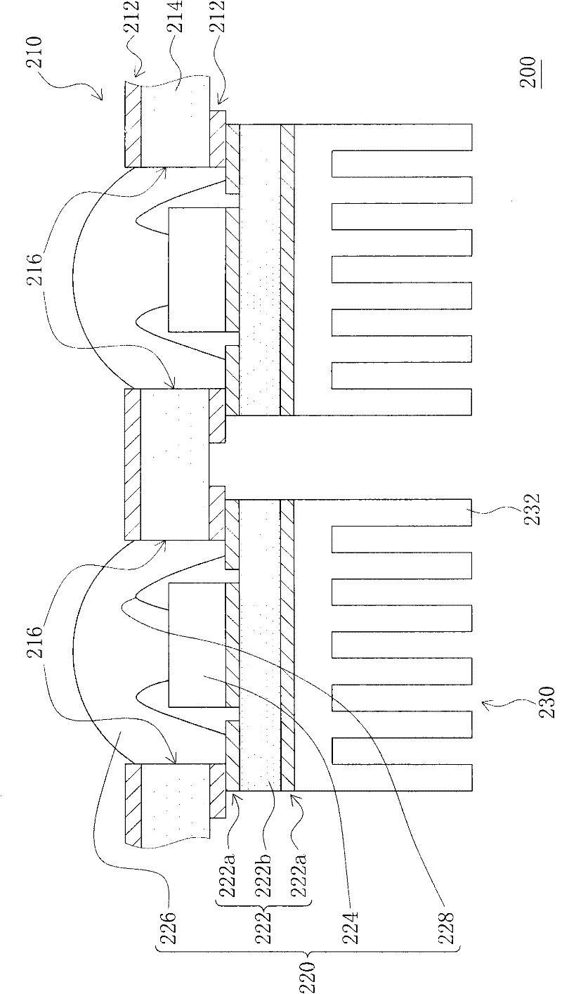
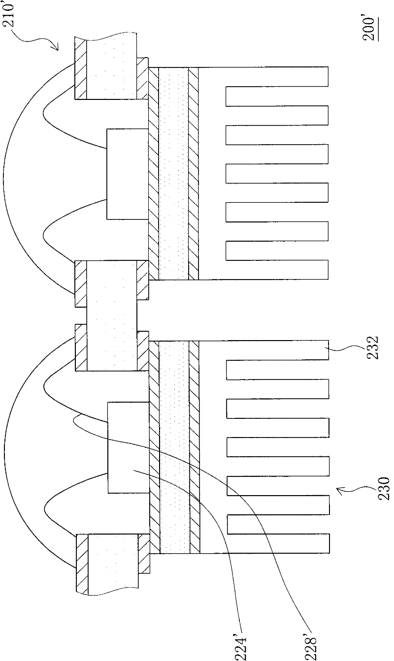
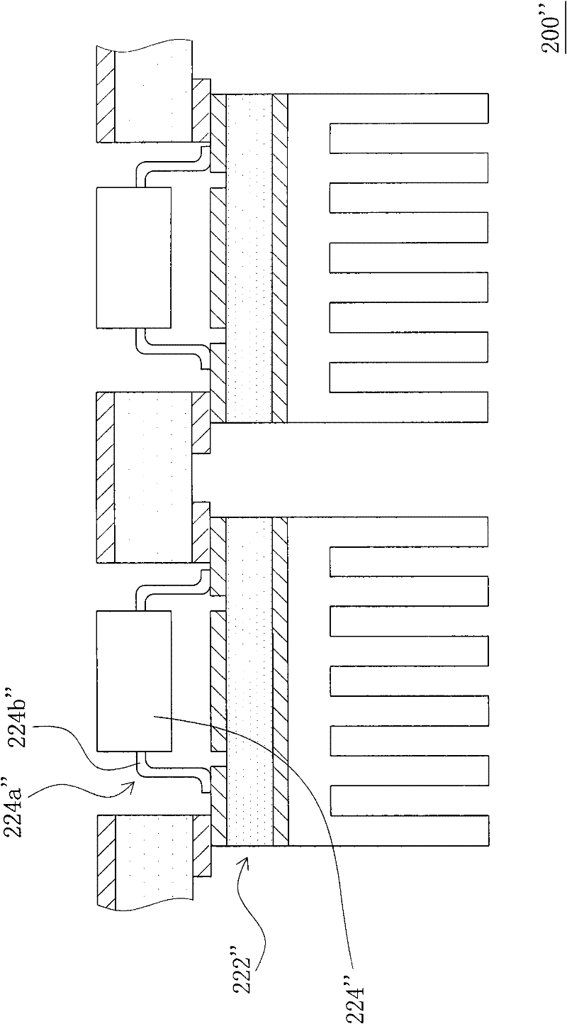
[0033] Figure 1A A schematic cross-sectional view of an electronic assembly according to the first group of embodiments of the present invention is shown. Please refer to Figure 1A The electronic assembly 200 of the first group of embodiments includes a first substrate 210, a plurality of electronic modules 220, and a plurality of heat dissipation devices 230. The first substrate 210 includes two first conductive layers 212 and a first insulating layer 214 and has a plurality of through holes 216. The first conductive layers 212 are respectively disposed on two opposite sides of the first insulating layer 214, and the material of each first conductive layer 212 is, for example, copper. In this embodiment, the first substrate 210 may have flexibility, and the material of the first insulating layer 214 is, for example, epoxy resin and polyimide (PI) resin. In addition, the number of the first conductive layers 212 and the number of the first insulating layers 214 in this embodiment are only for example and not for limiting the invention.
[0034] Each electronic module 220 includes a second substrate 222 and an electronic component 224. Each second substrate 222 is disposed on the first substrate 210 and includes two second conductive layers 222a and a second insulating layer 222b. The second conductive layers 222a are respectively disposed on opposite sides of the corresponding second insulating layer 222b, and the material of each second conductive layer 222a is, for example, copper or silver. The material of each second insulating layer 222b includes at least one of ceramic, diamond, graphite, and carbon-carbon composite material. In this embodiment, the material of each second insulating layer 222b includes ceramics, which includes at least one of aluminum oxide, zirconium oxide, silicon oxide, titanium oxide, aluminum nitride, silicon nitride, silicon carbide, and glass. For example, the material of each second insulating layer 222b is made up of 96% by weight aluminum oxide and 4% by weight magnesium oxide. In addition, the number of the second conductive layers 222a and the number of the second insulating layers 222b in this embodiment are only for example and not to limit the present invention. In addition, in another embodiment, the material of the first insulating layer 214 of the first substrate 210 may be aluminum oxide, and the material of the second insulating layer 222b of each second substrate 222 may be aluminum nitride.
[0035] It must be noted here that the thermal conductivity of each second insulating layer 222 b is greater than the thermal conductivity of the first insulating layer 214. In addition, the thermal expansion coefficient of each second insulating layer 222b may be less than the thermal expansion coefficient of the first insulating layer 214. The breakdown voltage of each second insulating layer 222b may be higher than the breakdown voltage of the first insulating layer 214. The electromagnetic wave interference resistance characteristics of each second insulating layer 222b may be better than the electromagnetic wave interference resistance characteristics of the first insulating layer 214. The electrostatic discharge resistance characteristics of each second insulating layer 222b may be better than the electrostatic discharge resistance characteristics of the first insulating layer 214. The radio frequency interference resistance characteristics of each second insulating layer 222 b may be better than the radio frequency interference resistance characteristics of the first insulating layer 214.
[0036] Each electronic component 224 is, for example, a chip, which is thermally connected to the corresponding second substrate 222. At least a part of each electronic component 224 is located in the corresponding through hole 216. In this embodiment, each electronic component 224, such as a chip, is electrically connected to one of the second conductor layers 222a of the corresponding second substrate 222 by wire bonding. In addition, each through hole 216 can be filled with a covering body 226, which can cover the electronic component 224 and the bonding wires 228. The light transmittance of the covering body 226 is not limited and the shape is not limited, and its function can be to protect the welding wires 228 from the influence of external moisture, heat and noise. In addition, if each electronic component 224 is a light emitting diode chip (LED chip), the cladding body 226 has light transmittance, and the shape of each through hole 216 can be changed according to design requirements to achieve the required light emission Mode and brightness requirements.
[0037] In another embodiment, each electronic component 224, such as a chip, may be electrically connected to the corresponding second substrate 222 by flip chip bonding. In addition, in another embodiment, each electronic component 224 may be a pre-packaged chip package, for example, a chip scale package (CSP), a wafer-level chip package (wafer-level chip). scale package (WLCSP) or stacked chip package (stacked chip package) and so on. However, the above is not shown in the drawings.
[0038] In detail, just Figure 1A In terms of relative position, each electronic component 224 is electrically connected to the second conductive layer 222a on the upper layer of the corresponding second substrate 222, which is located above the corresponding second insulating layer 222b. The upper second conductor layer 222 a of each second substrate 222 is electrically connected to the lower first conductor layer 212 of the first substrate 210. In other words, each electronic component 224 is electrically connected to the lower first conductor layer 212 of the first substrate 210 through the corresponding bonding wires 228 and the corresponding upper second conductor layer 222 a of the second substrate 222.
[0039] Each heat sink 230 is, for example, a heat sink, which is disposed on the second conductor layer 222a of the corresponding second substrate 222 and has a plurality of heat dissipation fins 232, so that each second substrate 222 Located between the corresponding electronic component 224 and the corresponding heat dissipation device 230. It must be noted here that the heat dissipation fins 232 of the heat dissipation devices 230 can be designed to be connected to a heat pipe (not shown). For example, the heat pipe passes through the heat dissipation fins 232 of the heat dissipation devices 230. The heat sink 230 and the heat pipe constitute a heat sink module. Therefore, heat can be transferred to the heat pipe by the heat dissipation fins 232 and quickly transferred to the external environment. In another embodiment, these heat dissipation devices 230 may be directly connected without a heat pipe to form another heat dissipation module. In other words, these heat dissipation devices 230 can be presented in the form of a shared heat dissipation module.
[0040] In this embodiment, when the electronic assembly 200 is operating, since the thermal conductivity of each second insulating layer 222b is greater than the thermal conductivity of the first insulating layer 214, the heat generated by each electronic component 224 can pass through the corresponding second substrate 222 and passed to the external environment. Therefore, compared with the prior art, the heat dissipation performance of the electronic assembly 200 of this embodiment is better. In addition, since the thermal expansion coefficient of each second insulating layer 222b may be less than the thermal expansion coefficient of the first insulating layer 214, each electronic component 224 disposed on the corresponding second substrate 222 is less susceptible to thermal expansion of the corresponding second substrate 222 Damage caused by the phenomenon. In addition, since the breakdown voltage of each second insulating layer 222b can be higher than the breakdown voltage of the first insulating layer 214, the electromagnetic wave interference resistance characteristics of each second insulating layer 222b can be better than that of the first insulating layer 214. The electrostatic discharge resistance characteristics of the second insulating layer 222b may be better than the electrostatic discharge resistance characteristics of the first insulating layer 214, or the radio frequency interference resistance characteristics of each second insulating layer 222b may be better than the radio frequency interference resistance of the first insulating layer 214 Therefore, the electrical efficiency of the second substrate 222 is better than that of the first substrate 210. Therefore, overall, the electrical performance of the electronic assembly 200 of this embodiment is better.
[0041] Figure 1B A schematic cross-sectional view of another electronic assembly according to the first group of embodiments of the present invention is shown. Please refer to Figure 1B The main difference between the electronic assembly 200' and the electronic assembly 200 is that each electronic component 224' of the electronic assembly 200' is electrically connected to the first substrate 210' through the corresponding bonding wires 228'.
[0042] Figure 1C A schematic cross-sectional view of another electronic assembly according to the first group of embodiments of the present invention is shown. Please refer to Figure 1C The main difference between the electronic assembly 200" and the electronic assembly 200 is that each electronic component 224" of the electronic assembly 200" is a chip package, and the lead frame 224a" of each electronic component 224" These leads 224b" are electrically connected to the corresponding second substrate 222".
[0043] [Second Group of Examples]
[0044] Figure 2A A schematic cross-sectional view of an electronic assembly according to the second group of embodiments of the present invention is shown. Please refer to Figure 2A The main difference between the electronic assembly 300 of the second group of embodiments and the electronic assembly 200 of the first group of embodiments is that at least a part of each heat dissipation device 330 is located in the corresponding through hole 316 of the first substrate 310. In addition, just Figure 2A In terms of relative position, the second conductor layer 322a of the lower layer of the second substrate 322 of each electronic module 320 is electrically connected to the first conductor layer 312 of the upper layer of the first substrate 310. In addition, each second substrate 322 may have a plurality of conductive through holes 322c, which penetrate the corresponding second insulating layer 322b and are electrically connected to the corresponding second conductive layers 322a. Each conductive through hole 322c may be formed with a conductive circuit in the through hole by copper paste sintering, silver paste sintering, chemical plating or sputtering.
[0045] Figure 2B A schematic cross-sectional view of another electronic assembly according to the second group of embodiments of the present invention is shown. Please refer to Figure 2B The main difference between the electronic assembly 300' and the electronic assembly 300 is that each electronic component 324' of the electronic assembly 300' is electrically connected to the first substrate 310' through the corresponding bonding wires 328'.
[0046] Figure 2C A schematic cross-sectional view of another electronic assembly according to the second group of embodiments of the present invention is shown. Please refer to Figure 2C The main difference between the electronic assembly 300" and the electronic assembly 300 is that each electronic component 324" of the electronic assembly 300" is a chip package, and the leads of the lead frame 324a" of each electronic component 324" 324b" is electrically connected to the corresponding second substrate 322".
[0047] Figure 2D A schematic cross-sectional view of another electronic assembly according to the second group of embodiments of the present invention is shown. Please refer to Figure 2D The main difference between the electronic assembly 300'” and the electronic assembly 300 is that each electronic component 324'” of the electronic assembly 300'” is a chip package, and the lead frame 324a' of each electronic component 324'” "These pins 324b'" are electrically connected to the first substrate 310'".
[0048] [Third set of examples]
[0049] Figure 3A A schematic cross-sectional view of an electronic assembly according to the third group of embodiments of the present invention is shown. Please refer to Figure 3A The main difference between the electronic assembly 400 of the third group of embodiments and the electronic assembly 200 of the first group of embodiments is that the first substrate 410 can omit the configuration of the through holes 216, and the number of heat dissipation devices 430 can be only One. The second substrate 422 of each electronic module 420 is disposed on the first substrate 410, and each second substrate 422 is located between the corresponding electronic component 424 and the first substrate 410. In addition, the first substrate 410 is located between each second substrate 422 and the heat dissipation device 430.
[0050] In this embodiment, each electronic component 424 is electrically connected to the first conductive layer 412 on the upper layer of the first substrate 410 through the corresponding bonding wires 428. In addition, the first substrate 410 may have a plurality of thermal through holes 418, which penetrate the first insulating layer 414, the thermally connected first conductor layers 412 and are located below the second substrates 422.
[0051] Figure 3B A schematic cross-sectional view of another electronic assembly according to the third group of embodiments of the present invention is shown. Please refer to Figure 3B The main difference between the electronic assembly 400' and the electronic assembly 400 is that each electronic component 424' of the electronic assembly 400' is electrically connected to the corresponding second substrate 422' through the corresponding bonding wires 428'.
[0052] Figure 3C A schematic cross-sectional view of another electronic assembly according to the third group of embodiments of the present invention is shown. Please refer to Figure 3C The main difference between the electronic assembly 400" and the electronic assembly 400 is that each electronic component 424" of the electronic assembly 400" is a chip package, and the leads of the lead frame 424a" of each electronic component 424" 424b" is electrically connected to the corresponding second substrate 422".
[0053] [Fourth group of embodiments]
[0054] Figure 4A A schematic cross-sectional view of an electronic assembly according to the fourth group of embodiments of the present invention is shown. Please refer to Figure 4A The main difference between the electronic assembly 500 of the fourth group of embodiments and the electronic assembly 200 of the first group of embodiments is that each electronic module 520 further includes a third substrate 521. Each third substrate 521 is located between the corresponding electronic component 524 and the first substrate 510. For example, each electronic component 524 of the chip is electrically connected to the corresponding third substrate 521 through a plurality of bumps 528. That is, each electronic component 524 is electrically connected to the corresponding third substrate 521 through flip chip bonding. In addition, the third substrate 521 is electrically connected to the first conductive layer 512 of the upper layer of the first substrate 510 through a plurality of solder balls 523. These solder balls 523 may be ball grid array (BGA) type input and output interfaces. In summary, each electronic component 524 is electrically connected to the first substrate 510 through the third substrate 521.
[0055] It must be noted here that for one of the electronic modules 520, for example, the electronic component 524 of the chip, the corresponding bumps 528, the corresponding solder balls 523, and the corresponding third substrate 521 may be formed in advance. A chip package.
[0056] In addition, each second substrate 522 is located between the corresponding electronic component 524 and the corresponding heat dissipation device 530. Each electronic component 524 is thermally connected to the corresponding heat sink 530 through the corresponding second substrate 522. Each second substrate 522 can serve as a buffer between the corresponding electronic component 524 with a lower coefficient of thermal expansion and the corresponding heat sink 530 with a higher coefficient of thermal expansion.
[0057] Figure 4B A schematic cross-sectional view of another electronic assembly according to the fourth group of embodiments of the present invention is shown. Please refer to Figure 4B The main difference between the electronic assembly 500' and the electronic assembly 500 is that each electronic component 524' of the electronic assembly 500' is a chip package, and the leads of the lead frame 524a' of each electronic component 524' 524b' is electrically connected to the first substrate 510'.
[0058] In summary, the electronic assembly of the embodiment of the present invention has at least one of the following or other advantages:
[0059] 1. When the electronic assembly of the embodiment of the present invention operates, since the thermal conductivity of the second insulating layer is greater than the thermal conductivity of the first insulating layer, the heat generated by the electronic component can be transferred to the external environment through the second substrate. Therefore, compared with the prior art, the electronic assembly of the embodiment of the present invention has better heat dissipation performance.
[0060] 2. Since the thermal expansion coefficient of the second insulating layer can be smaller than that of the first insulating layer, in the embodiment of the present invention, the electronic components arranged on the second substrate are less susceptible to the thermal expansion phenomenon of the second substrate And produce damage.
[0061] 3. Since the breakdown voltage of the second insulating layer can be higher than the breakdown voltage of the first insulating layer, the electromagnetic wave resistance of the second insulating layer can be better than that of the first insulating layer, and the second insulating layer is resistant to static electricity The discharge characteristics can be better than the electrostatic discharge resistance of the first insulating layer, or the radio frequency interference resistance of the second insulating layer can be better than the radio frequency interference resistance of the first insulating layer, so the second substrate has better electrical performance Electrical performance on the first substrate. Therefore, overall, the electrical performance of the electronic assembly of the embodiment of the present invention is better.
[0062] The above are only the embodiments of the present invention, and do not limit the present invention in any form. Although the present invention has been disclosed as above by the embodiments, it is not intended to limit the present invention. Anyone familiar with the field, Without departing from the scope of the technical solution of the present invention, when the above-disclosed technical content can be used to make slight changes or modification into equivalent embodiments with equivalent changes, as long as it does not depart from the technical solution content of the present invention, the technical essence of the present invention is used to compare the above Any simple modifications, equivalent changes and modifications made in the embodiments still fall within the scope of the technical solutions of the present invention.