Bipolar CMOS DMOS (BCD) integrated device based on N type extension layer and manufacture method thereof

A technology for integrating devices and epitaxial layers, which is applied in semiconductor/solid-state device manufacturing, electrical solid-state devices, semiconductor devices, etc., can solve the problems of increasing the cost of silicon wafers, reduce resistivity, avoid the increase of chip manufacturing costs, and reduce manufacturing costs. cost effect

Inactive Publication Date: 2011-09-28
UNIV OF ELECTRONICS SCI & TECH OF CHINA
View PDF2 Cites 20 Cited by
  • Summary
  • Abstract
  • Description
  • Claims
  • Application Information

AI Technical Summary

Problems solved by technology

In order to improve the vertical body withstand voltage of the device, high-resistivity silicon wafers are usually used as substrates, but high-resistance wafers (>100Ω·cm) are usually manufactured by zone melting, which increases the cost of silicon wafers

Method used


Image

  • Bipolar CMOS DMOS (BCD) integrated device based on N type extension layer and manufacture method thereof
  • Bipolar CMOS DMOS (BCD) integrated device based on N type extension layer and manufacture method thereof
  • Bipolar CMOS DMOS (BCD) integrated device based on N type extension layer and manufacture method thereof

Examples


Embodiment Construction

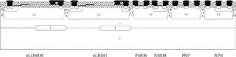
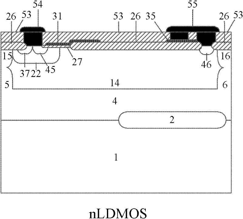
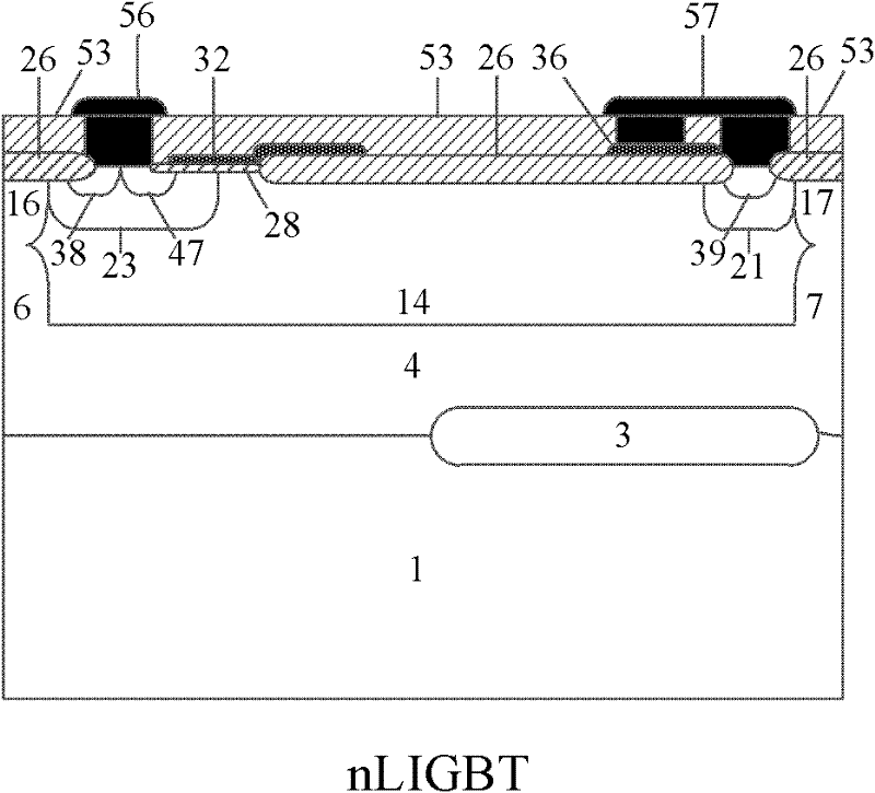
[0027] The present invention provides a BCD integrated device based on an N-type epitaxial layer, such as figure 1 As shown, it includes high-voltage nLDMOS devices, high-voltage nLIGBT devices, low-voltage PMOS devices, low-voltage NMOS devices, low-voltage PNP devices, and low-voltage NPN devices integrated on the same P-type substrate 1. The high-voltage nLDMOS device, high-voltage nLIGBT device, low-voltage PMOS device, low-voltage NMOS device, low-voltage PNP device, and low-voltage NPN device are fabricated in the N-type epitaxial layer 14 on the surface of the P-type epitaxial layer 4 on the surface of the P-type substrate 1, and pass P + To achieve junction isolation in the isolation regions 5-10 and 15-20. There is a first N-type buried layer 2 between the P-type substrate 1 and the P-type epitaxial layer 4 under the high-voltage nLDMOS device, and a second N-type buried layer 2 is provided between the P-type substrate 1 and the P-type epitaxial layer 4 under the high-v...


PUM


Abstract

A bipolar CMOS DMOS (BCD) integrated device based on a N type extension layer and a manufacture method thereof, which belongs to the semiconductor power device technology field, are disclosed. In the invention, a high voltage nLDMOS device, a high voltage nLIGB device, a low voltage PMOS device, a low voltage NMOS device, a low voltage PNP device and a low voltage NPN device are integrated on a same substrate. All devices are made in an N type extension layer arranged on a surface of a P type extension layer which is on a surface of a P type substrate. And junction isolations of the devices are realized through P<+> isolation regions. N type buried layers are arranged between the P type substrate and the P type extension layer, wherein the P type substrate and the P type extension layer are under the high voltage devices. N type buried layers are/ are not arranged between the P type extension layer and the N type extension layer, wherein the P type extension layer and the N type extension layer are under the low voltage devices. The N type buried layers are introduced in the invention to realize that silicon chips with lower resistivity can be used as the substrate at a same breakdown voltage. In the prior art, float-zone technique is adopted to manufacture monocrystalline silicon pieces, which can increase the chip manufacturing costs. In the invention, the float-zone technique is not used so that the chip manufacturing costs can be reduced.

Description

Technical field [0001] The invention belongs to the technical field of semiconductor power devices. Background technique [0002] BCD (Bipolar CMOS DMOS) process technology utilizes the high analog accuracy of Bipolar transistors, the high integration of CMOS and the high power characteristics of DMOS (Double-diffused MOSFET) to realize Bipolar analog circuits, CMOS logic circuits, CMOS analog circuits and DMOS high voltage Monolithic integration of power devices. Lateral high voltage power devices LDMOS (Lateral Double-diffused MOSFET) and LIGBT (Lateral Insulated Gate Bipolar Trasistor) are easily compatible with traditional CMOS devices, so they have been widely used in the field of smart power integrated circuits. The primary purpose of the design of a horizontal high voltage power device is to achieve a rated breakdown voltage under a given drift zone length, and its breakdown voltage is determined by the lowest value of the lateral surface withstand voltage and the longitu...

Claims


Application Information

Patent Timeline
Patent Type & Authority Applications(China)
IPC IPC(8): H01L27/06H01L29/78H01L29/06H01L21/8249
Inventor 乔明银杉赵远远章文通温恒娟向凡周锌
Owner UNIV OF ELECTRONICS SCI & TECH OF CHINA
Why Eureka
Try Eureka