High density integrated circuit module structure

An integrated circuit and module structure technology, which is applied to circuits, electrical components, electrical solid devices, etc., can solve the problems of inapplicability, poor heat dissipation of the integrated circuit module structure 100, and reduced manufacturing costs, and achieves a simple, convenient and good assembly process. The effect of signal transmission quality, lower manufacturing cost

Inactive Publication Date: 2011-10-05
WALTON ADVANCED ENG INC
View PDF3 Cites 10 Cited by
  • Summary
  • Abstract
  • Description
  • Claims
  • Application Information

AI Technical Summary

Problems solved by technology

The first chip 112 is flip-chip bonded on the first substrate 111 through the first bumps 113, and the second chip 122 is flip-chip bonded on the second substrate 121 through the second bumps 123. In order to increase the function of the product, The first package 110 and the second package 120 must be stacked, and then the first package 110 and the second package 120 are electrically connected through the carrier board 130, each first solder ball 114 and each second solder ball 124, However, in the integrated circuit module structure 100, in order to realize electrical connection between the first package 110 and the second package 120, it is necessary to reserve the space for the carrier board 130, each first solder ball 114 and each second solder ball 124, so it is impossible to Reducing the thickness of the integrated circuit module structure 100 cannot be applied to electronic products with light, thin, short, small and other miniature memory
In addition, the first package 110 is electrically connected to the second package 120 through the carrier board 130, the first solder balls 114 and the second solder balls 124, resulting in the need to pass through the first solder balls during the manufacturing process. 114 and each second solder ball 124 contact steps, so it is impossible to reduce the related assembly process and reduce the manufacturing cost
In addition, when the integrated circuit module structure 100 is subjected to stress, the first solder balls 114 and the second solder balls 124 may be easily damaged due to vibration factors, resulting in poor signal transmission quality.
Even, since the first chip 112 and the second chip 122 will generate high temperature during operation, it is easy to cause the problem of poor heat dissipation in the integrated circuit module structure 100

Method used


Image

  • High density integrated circuit module structure
  • High density integrated circuit module structure
  • High density integrated circuit module structure

Examples


Embodiment Construction

[0031] In order to make the purpose, features and functions of the present invention more comprehensible, the present invention will be described in detail with reference to the following embodiments and accompanying drawings.

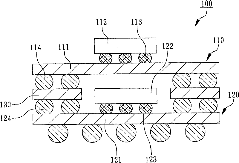
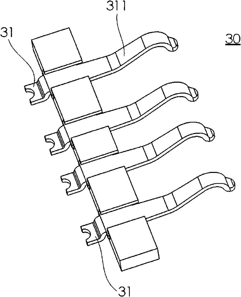
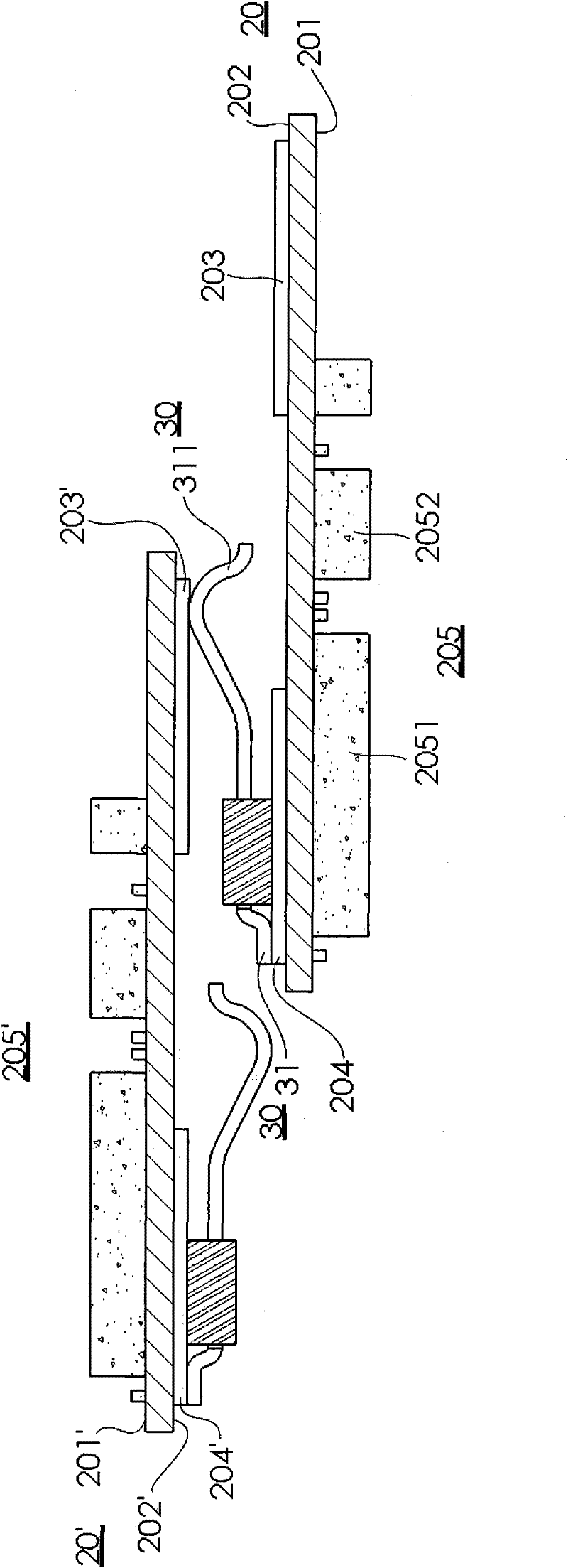
[0032] Such as figure 2 , image 3As shown, it is a high-density integrated circuit module structure provided by the present invention, which mainly includes at least one substrate 20 and at least one heat dissipation element 30 . The substrate 20 is used as a chip carrier and a transfer interface. It has an inner surface 201 and an outer surface 202 . It may be a high-density double-sided multilayer printed circuit board with circuits (not shown) formed inside. Wherein, the outer surface 202 has a plurality of outer contact pads 203 and a plurality of transfer contact pads 204, wherein the outer contact pads 203 and the transfer contact pads 204 are arranged in reverse symmetry, and the outer contact pads 203 pass through the circuit on the substrat...


PUM


Abstract

The invention relates to a high density integrated circuit module structure which comprises the following components: at least one substrate which has an interior surface and an external surface, wherein the external surface is provided with a plurality of external contact pads and a plurality of switch contact pads, the external contact pads connect the switch contact pads, the inner surface of the substrate is provided with at least one electronic component which connects the external contact pads and the switch contact pads; and at least one heat radiation component which comprises a plurality of thermal conductors, wherein the heat radiation component is arranged on a substrate surface which is provided with a plurality of switch contact pads, the thermal conductors connect the switch contact pads, the thermal conductors are provided with at least one uneven structure. The external contact pads of the substrate connect switch contact pads of another substrate through a plurality of thermal conductors, thus the integrated circuit displays a reverse interleaved contact high density stack structure. The high density integrated circuit module structure has an electronic product expansion function within a limited height, good vibration-proof capability and heat radiation effect, simple and convenient assembly operation, and efficacy of manufacture cost reduction.

Description

technical field [0001] The invention relates to an integrated circuit module structure, in particular to a high-density integrated circuit module structure. Background technique [0002] Such as figure 1 As shown, the conventional integrated circuit module structure 100 includes a first package 110 , a second package 120 and a carrier 130 . The first package 110 includes a first substrate 111 , a first chip 112 , a plurality of first bumps 113 and a plurality of first solder balls 114 . The second package 120 includes a second substrate 121 , a second chip 122 , a plurality of second bumps 123 and a plurality of second solder balls 124 . The first chip 112 is flip-chip bonded on the first substrate 111 through the first bumps 113, and the second chip 122 is flip-chip bonded on the second substrate 121 through the second bumps 123. In order to increase the function of the product, The first package 110 and the second package 120 must be stacked, and then the first package ...

Claims


Application Information

Patent Timeline
Patent Type & Authority Applications(China)
IPC IPC(8): H01L25/18H01L23/48H01L23/12H01L23/367
CPCH01L2224/16225H01L2924/0002H01L2924/15311
Inventor 于鸿祺
Owner WALTON ADVANCED ENG INC
Why Eureka
Try Eureka