Resistive random access memory using electric field enhancing layer and preparation method thereof

A technology of resistive variable memory and electric field enhancement, which is applied in the direction of electric solid-state devices, circuits, electrical components, etc., can solve the problems that the memory is easy to lose data, thin, and it is difficult to break through the bottleneck of the flash memory, so as to solve the problems of unstable performance, performance Stable and controllable effect

Inactive Publication Date: 2011-10-05
FUDAN UNIV
View PDF2 Cites 8 Cited by
  • Summary
  • Abstract
  • Description
  • Claims
  • Application Information

AI Technical Summary

Problems solved by technology

[0002] With the continuous shrinking of integrated circuit process technology nodes, traditional flash memory (Flash) non-volatile memory cannot be thinned indefinitely with the development of integrated circuit technology because of its floating gate, and it is difficult for flash memory to break through the 45nm process Bottleneck, in addition, dynamic and static memory are easy to lose data after power failure

Method used


Image

  • Resistive random access memory using electric field enhancing layer and preparation method thereof
  • Resistive random access memory using electric field enhancing layer and preparation method thereof
  • Resistive random access memory using electric field enhancing layer and preparation method thereof

Examples


Embodiment Construction

[0021] The present invention will be further described in detail below in conjunction with the accompanying drawings and specific embodiments. In the drawings, for the convenience of illustration, the thicknesses of layers and regions are enlarged or reduced, and the sizes shown do not represent actual sizes. Although these figures do not fully reflect the actual size of the device, they still completely reflect the mutual positions between the regions and the constituent structures, especially the upper-lower and adjacent relationships between the constituent structures.

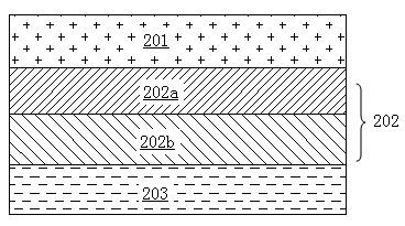
[0022] figure 2 A cross-sectional view of an embodiment of a performance controllable resistive memory provided by the present invention, such as figure 2 As shown, the RRAM includes a top electrode 201, a bottom electrode 203, and a composite dielectric layer 202 between the top electrode 201 and the bottom electrode 203. The composite dielectric layer 202 includes a resistance transition layer (usually ...


PUM


Abstract

The invention belongs to the technical field of non-volatile memories, in particular relates to a resistive random access memory using an electric field enhancing layer and a manufacturing method thereof. The resistive random access memory provided by the invention comprises a top electrode, a bottom electrode as well as a resistance-variable functional medium layer and an electric field enhancing layer, wherein the resistance-variable functional medium layer and the electric field enhancing layer are positioned between the top electrode and the bottom electrode; the electric field enhancing layer and a resistance conversion type memory are adjacent to each other; moreover, the dielectric constant of the electric field enhancing layer is lower than that of the resistance-variable functional medium layer. In the invention, resistance-variable functional materials with different dielectric constants are selected to form a laminated structure so as to adjust electric field distribution in a resistive random access memory structural unit so that the conductive channels formed on the resistive random access memory in the resistance varying process are controlled in structure and number through controlling the electric field distribution. The performance of the resistive random access memory provided by the invention is stable and controllable.

Description

technical field [0001] The invention belongs to the technical field of non-volatile memory, and in particular relates to a resistive variable memory and a manufacturing method thereof. Background technique [0002] With the continuous shrinking of integrated circuit process technology nodes, traditional flash memory (Flash) non-volatile memory cannot be infinitely thinned with the development of integrated circuit technology because of its floating gate, and it is difficult for flash memory to break through the 45nm process Bottleneck, in addition, dynamic and static memory are easy to lose data after power failure. In recent years, various new types of non-volatile memory have been developed rapidly, such as ferroelectric memory (FRAM), magnetic memory (MRAM), phase change memory (PRAM) and resistive change memory (RRAM). [0003] Among these memories, the information read and write of the resistive variable memory is realized by reading or changing the resistance of the r...

Claims


Application Information

Patent Timeline
Patent Type & Authority Applications(China)
IPC IPC(8): H01L45/00H01L27/24
Inventor 张卫陈琳周鹏孙清清王鹏飞
Owner FUDAN UNIV
Why Eureka
Try Eureka