WOLED (white organic light-emitting device) and manufacturing method thereof

An electroluminescent device, organic technology, applied in chemical instruments and methods, semiconductor/solid-state device manufacturing, luminescent materials, etc., can solve the problems of increased difficulty in device structure and manufacturing process, reduce luminescence quenching, and improve utilization efficiency and reduce energy loss

Inactive Publication Date: 2013-10-16
UNIV OF ELECTRONICS SCI & TECH OF CHINA
View PDF3 Cites 0 Cited by
  • Summary
  • Abstract
  • Description
  • Claims
  • Application Information

AI Technical Summary

Problems solved by technology

Among them, for example, in the patent CN201010198948.4, the host material and the blue dopant are co-evaporated from two sources, and finally the host material, the blue dopant, and the red dopant are co-evaporated from three sources. Increased corresponding difficulty in structure and manufacturing process

Method used


Image

  • WOLED (white organic light-emitting device) and manufacturing method thereof
  • WOLED (white organic light-emitting device) and manufacturing method thereof
  • WOLED (white organic light-emitting device) and manufacturing method thereof

Examples


Embodiment 1

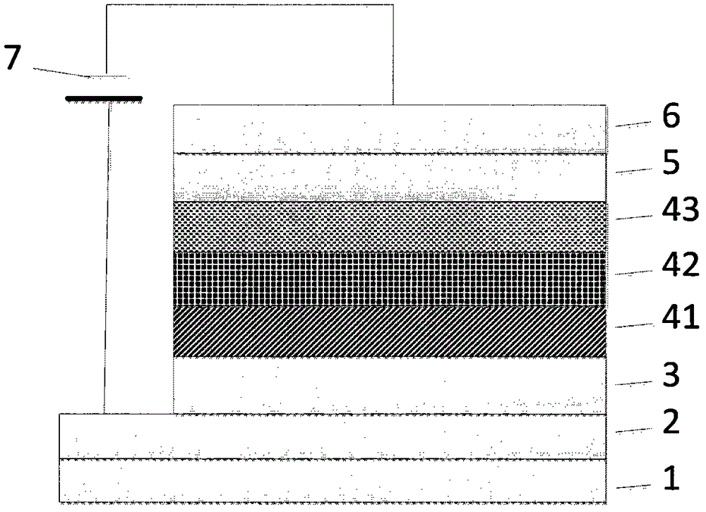
[0064] Such as figure 2 As shown, the substrate 1 of the device is a glass substrate, the anode layer 2 is ITO, the hole transport material 3 is NPB, the electron transport material 5 is Bphen, the complementary phosphorescent material 41 is tbt, and the hole transport and energy transfer material 42 is mCP, the single doping material 43 is FIr6, the main material is UGH2, and the cathode layer 6 is Mg:Ag alloy. The entire device structure is described as:

[0065] Glass substrate / ITO / NPB / tbt(0.1nm) / mCP / UGH2:10%FIr6(20nm) / Bphen / Mg:Ag(200nm)

[0066] The preparation method is as follows:

[0067] ①Use detergent, ethanol solution, deionized water and alcohol to ultrasonically clean the transparent conductive substrate ITO glass, and dry it with dry nitrogen after cleaning. Wherein the ITO film on the glass substrate is used as the anode layer of the device, the square resistance of the ITO film is 10Ω / sq, and the film thickness is 180nm.

[0068] ②The dried substrate was mo...

Embodiment 2

[0077] Such as figure 2 As shown, the substrate 1 of the device is a glass substrate, the anode layer 2 is ITO, the hole transport material 3 is NPB, and the complementary phosphorescent material 41 in the structure of the device is (pbi) 2 Ir(acac), the hole transport and energy transfer material 42 is mCP, the single doping material 43 is FIrpic, the host material is UGH2, the electron transport material 5 is Bphen, and the cathode layer 6 is Mg:Ag alloy. The entire device structure is described as:

[0078] Glass substrate / ITO / NPB / (pbi) 2 Ir(acac)(1nm) / mCP / UGH2:10%FIrpic(20nm) / Bphen / Mg:Ag(200nm)

[0079] The fabrication process of the device is similar to that of Example 1.

Embodiment 3

[0081] Such as figure 2 As shown, the substrate 1 of the device is a glass substrate, the anode layer 2 is ITO, the hole transport material 3 is NPB, and the complementary phosphorescent material 41 in the structure of the device is (tpbi) 2 Ir(acac), the hole transport and energy transfer material 42 is mCP, the single doping material 43 is FIr6, the host material is UGH2, the electron transport material 5 is Bphen, and the cathode layer 6 is Mg:Ag alloy. The entire device structure is described as:

[0082] Glass substrate / ITO / NPB / (tpbi) 2 Ir(acac)(2nm) / mCP / UGH2:10%FIr6(20nm) / Bphen / Mg:Ag(200nm)

[0083] The fabrication process of the device is similar to that of Example 1.


PUM

PropertyMeasurementUnit
thicknessaaaaaaaaaa
thicknessaaaaaaaaaa

Abstract

The invention provides a WOLED (white organic light-emitting device) using double-fluorescent dyes to evaporate in different modes and a manufacturing method thereof. The WOLED structure comprises a substrate, a first electrode layer on a substrate surface, a functional layer on the first electrode layer and a second electrode layer on the functional layer, wherein the functional layer at least comprises an EML (emission layer), an ETL (electron transport layer) and an HTL (hole transport layer); and the EML is a combined layer which is evaporated by blue phosphorescent materials and complementary phosphorescent materials in a doped mode and a thin film mode respectively. Compared with other white devices, the energy efficiency and the current efficiency of the WOLED are improved greatly. By adopting the manufacturing method, the WOLED can be used to replace a traditional complicated multilayer doping and codoping white organic device, and the processes and procedures of manufacturing the device can be simplified. The luminescence is stable, the control is easy and the repeatability is good.

Description

technical field [0001] The invention relates to the technical field of organic electroluminescent devices, in particular to a white light organic electroluminescent device and a preparation method thereof. Background technique [0002] With the rapid development of science and technology, information display has become an important field in today's society. The current display technology is mainly represented by liquid crystal display, but it has shortcomings in terms of viewing angle, power consumption, response speed, and high and low temperature characteristics. At the same time, with the aggravation of the global warming effect and the increasing depletion of fossil energy, energy conservation and emission reduction have been put on the agenda, so people pay great attention to high-efficiency lighting devices and light sources, such as energy-saving lamps, which are widely used at present, but their It has the disadvantages of low efficiency and polluting the environment...

Claims


Application Information

Patent Timeline
Patent Type & Authority Patents(China)
IPC IPC(8): H01L51/50H01L51/52H01L51/54H01L51/56C09K11/06
CPCY02B20/00
Inventor 于军胜刘胜强黄江蒋亚东
Owner UNIV OF ELECTRONICS SCI & TECH OF CHINA
Why Eureka
Try Eureka