Packaging method possessing wafer dimension plaster

A technology of wafer size and packaging method, used in electrical components, circuits, semiconductor/solid-state device manufacturing, etc. Heat dissipation performance, effect of size reduction

Active Publication Date: 2013-11-06
重庆万国半导体科技有限公司
View PDF7 Cites 0 Cited by
  • Summary
  • Abstract
  • Description
  • Claims
  • Application Information

AI Technical Summary

Problems solved by technology

In this packaging, the wafer is cut from the beginning, and then the electrodes of the semiconductor elements are connected and packaged. Wrapped in the package, the heat dissipation performance of the semiconductor element is deteriorated

Method used


Image

  • Packaging method possessing wafer dimension plaster
  • Packaging method possessing wafer dimension plaster
  • Packaging method possessing wafer dimension plaster

Examples


Embodiment Construction

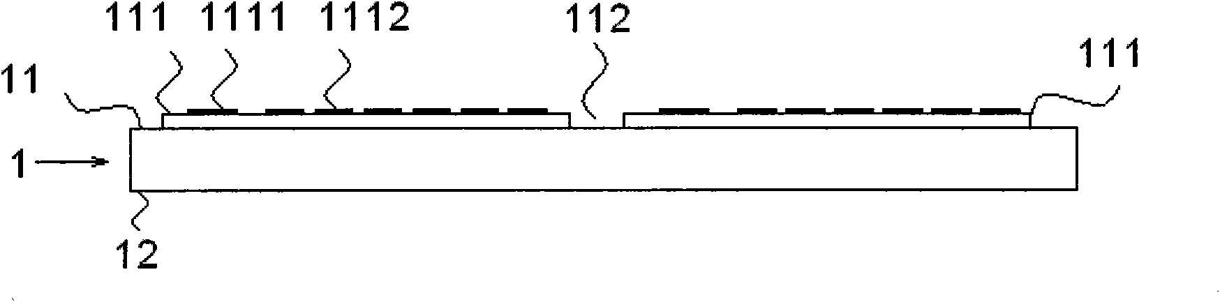
[0050] The present invention provides a package with wafer size patch, which includes a wafer 1 , a patch 2 and a plastic package 3 .

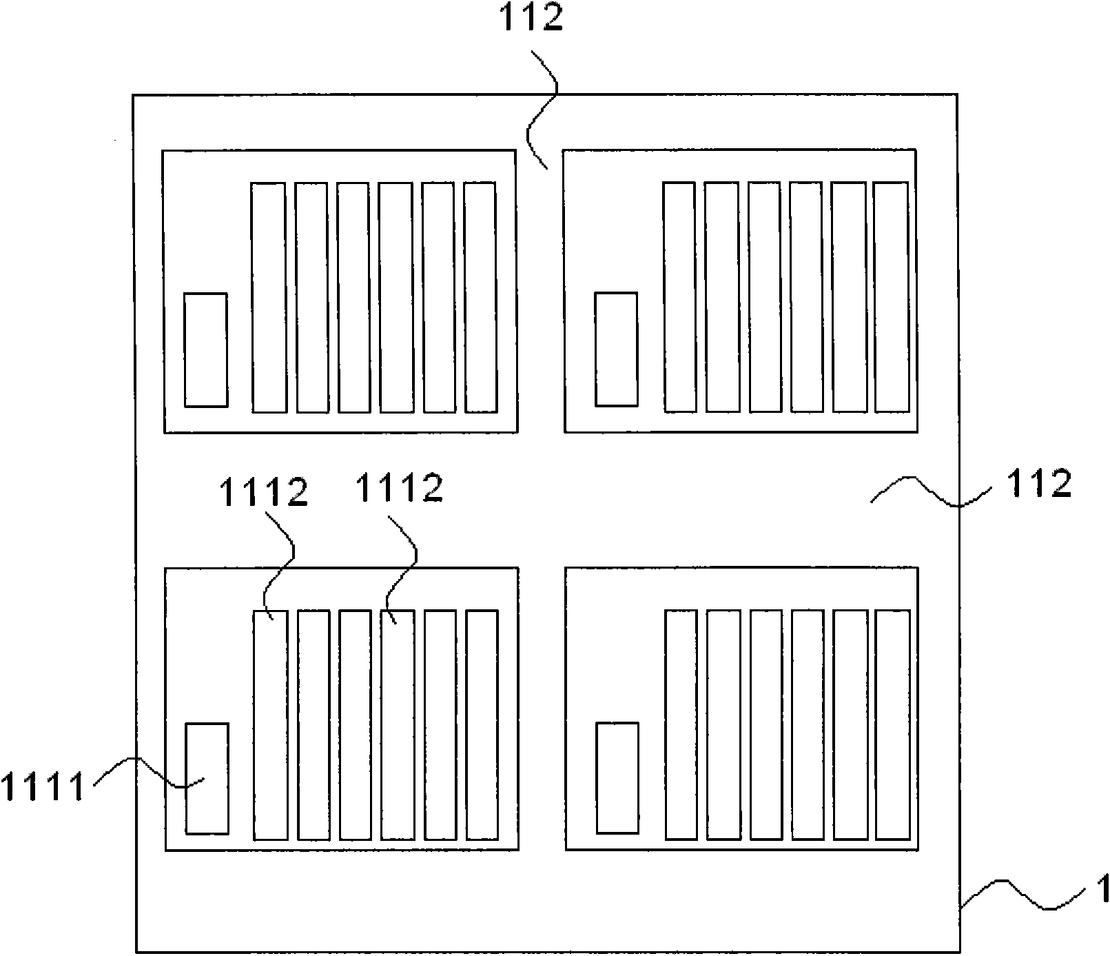
[0051] like Figure 1A ,1B Shown are a side view of the wafer and a front view of the top of the wafer, respectively, with wafer 1 having a wafer top 11 and a wafer bottom 12 . Several chips 111 are produced on the top of the wafer 11, and recessed areas 112 are arranged between the chips 111 on the top of the wafer 11, each chip 111 corresponds to a recessed area 112, and adjacent recessed areas can be separated , can also extend the connection. In a preferred embodiment, the groove area 112 divides the several chips 111 into chip units in both vertical and horizontal directions between the chips 111 . In another preferred embodiment, the recessed area 112 is only provided in one direction (not shown in the figure). The upper surface of each chip is provided with several chip top electrode contact areas 1111 and 1112 . When the area of ​​t...


PUM


Abstract

The invention discloses a packaging method possessing wafer dimension paster. The method is characterized in that a wafer, a paster and a plastic-sealed body are included, wherein the wafer comprises a wafer top and a wafer bottom, a plurality of chips are made on the wafer top, a groove area is provided among the chips on the wafer top, the groove area divides the chips into some chip units, the surface of each chip unit is provided with a chip top contact zone, the paster is provided with areas corresponding to each chip unit on the wafer, the paster possesses a plurality of paster contact zones and paster connection ribs, the paster connection ribs are provided in the groove area, the plastic-sealed body plastically packs the wafer top, the chips and the paster, it is required to grind or cut the wafer bottom to a whole packaging body so as to expose the chip electrodes and the packaging body needs to be cut. According to the invention, the process flow of the packaging is simplified, the packaging volume of the chips is reduced, the packaging cost is reduced and the heat radiation performance of the chips is improved.

Description

technical field [0001] The invention relates to a semiconductor packaging method, in particular to a packaging method with wafer size patching. Background technique [0002] In the process of semiconductor manufacturing, multiple circuit structures are usually fabricated on one wafer, then the wafer is cut, the wafer is divided into individual chips, and then each chip is connected to the substrate through packaging processes such as patch welding for various products. production. [0003] For example, Chinese Patent Publication No. CN 1945805A discloses a semiconductor packaging method, which includes the following steps: first, providing a circuit substrate having a first surface and a second surface. Next, a solvent-free double-stage thermosetting compound is formed on the first surface of the circuit substrate. Then, the solvent-free double-stage thermosetting compound is partially cured to form a solvent-free B-stage adhesive layer on the first surface of the circuit ...

Claims


Application Information

Patent Timeline
Patent Type & Authority Patents(China)
IPC IPC(8): H01L21/50H01L21/60H01L21/78
Inventor 龚玉平
Owner 重庆万国半导体科技有限公司
Why Eureka
Try Eureka