LED (light-emitting diode) light source module and packaging process thereof

An LED light source, LED chip technology, applied in electrical components, electrical solid devices, circuits, etc., can solve the problems of complex circuit connections, difficult to meet the requirements of light color uniformity and heat dissipation performance, achieve uniform light color, reduce open circuits, Good heat dissipation effect

Inactive Publication Date: 2011-10-19
DONGGUAN BANGCHEN PHOTOELECTRIC
View PDF7 Cites 7 Cited by
  • Summary
  • Abstract
  • Description
  • Claims
  • Application Information

AI Technical Summary

Problems solved by technology

The current large LED display system is made of dot matrix templates, usually 8X8 or 16X16 circuit boards. The larger the screen, the more templates are needed,

Method used


Image

  • LED (light-emitting diode) light source module and packaging process thereof
  • LED (light-emitting diode) light source module and packaging process thereof
  • LED (light-emitting diode) light source module and packaging process thereof

Examples


Example Embodiment

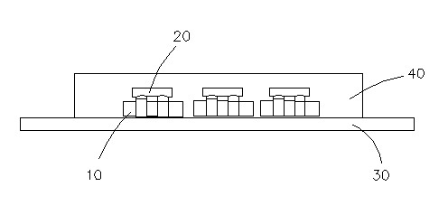
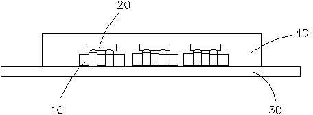
[0012] In order to further understand the features, technical means, and specific goals and functions of the present invention, the present invention will be described in further detail below with reference to the accompanying drawings and specific embodiments.

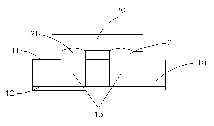
[0013] see figure 1 and figure 2 The LED light source module of the present invention includes a plurality of light source units and a substrate 30 . The light source unit includes a silicon wafer 10 and a chip array 20 .

[0014] see figure 2 The silicon wafer 10 is made of insulating materials such as ceramics. The silicon wafer 10 includes an upper surface 11 and a welding surface 12 . The upper surface 11 is provided with a circuit. The silicon wafer 10 is provided with a number of through holes 13 . The chip array 20 includes a plurality of LED chips 21 . The LED chips 21 are soldered on the through holes 13 , and the LED chips 21 are connected to the circuits on the upper surface 11 and the soldering surface...


PUM


Abstract

The invention discloses an LED (light-emitting diode) light source module, which comprises a plurality of light source cells and a substrate. Each light source cell comprises a silicon chip and a chip array; the silicon chip is arranged on the substrate; the chip array is arranged on the silicon chip; the silicon chip comprises an upper surface and a welding face; a circuit is arranged on the upper surface; the silicon chip is provided with a conducting hole; an LED chip is welded on the conducting hole; and the LED chip is connected with the circuit on the upper surface and the welding face. By coating fluorescent powder on the substrate, the LED light source module disclosed by the invention has evener light color; by directly adhering the LED chip welded with the silicon chip on the substrate, the occurrence of open circuit and short circuit is reduced, and heat radiation performance is good, and the packaging is convenient.

Description

technical field [0001] The invention relates to an LED light source module, in particular to an LED light source module and a packaging process thereof. Background technique [0002] Human society is entering the era of optoelectronics. It is estimated that from 2010 to 2015, the electronic industry will replace the traditional electronic industry and become the largest industry in the 21st century. It will also become an important indicator of a country's economic development and comprehensive national strength. At present, as a kind of photoelectric product, LED large-screen electronic display has attracted people's attention day by day. It can display or loop text, graphics and image information in real time. It has many advantages such as rich display methods, strong ornamental value, convenient display content modification, high brightness, stable display and long life. It is widely used in commercial advertisements and sports competitions. It is one of the powerful to...

Claims


Application Information

Patent Timeline
IPC IPC(8): H01L25/075H01L33/62H01L33/00
Inventor 徐朝丰
Owner DONGGUAN BANGCHEN PHOTOELECTRIC
Why Eureka
Try Eureka