Method for designing AES (Advanced Encryption Standard) encryption chip based on FPGA (Field Programmable Gate Array) and embedded encryption system

A technology of encryption chip and design method, which is applied in the direction of encryption device with shift register/memory, etc., can solve the problem of communication error detection without considering the problem of AES operation mode

Inactive Publication Date: 2011-10-19
BEIHANG UNIV
View PDF4 Cites 63 Cited by
  • Summary
  • Abstract
  • Description
  • Claims
  • Application Information

AI Technical Summary

Problems solved by technology

[0007] After searching the literature of the prior art, it was found that the Chinese patent "Design method of AES encryption chip and computer encryption machine", publication number CN 10626289A, the patent on January 13, 2010, is an encryption designed for computer encryptio

Method used


Image

  • Method for designing AES (Advanced Encryption Standard) encryption chip based on FPGA (Field Programmable Gate Array) and embedded encryption system
  • Method for designing AES (Advanced Encryption Standard) encryption chip based on FPGA (Field Programmable Gate Array) and embedded encryption system
  • Method for designing AES (Advanced Encryption Standard) encryption chip based on FPGA (Field Programmable Gate Array) and embedded encryption system

Examples


Embodiment Construction

[0067] The specific embodiment of the present invention will be described in further detail in conjunction with the accompanying drawings.

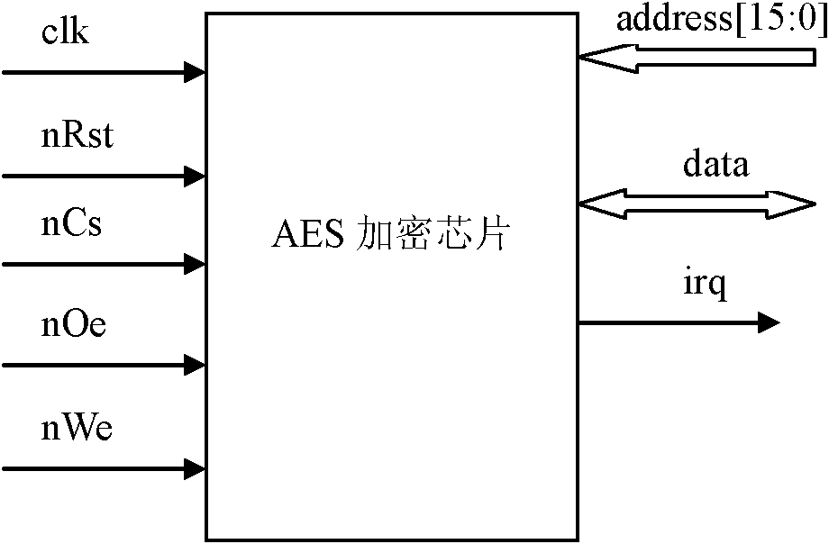
[0068] First, describe the main external signals of the AES encryption chip, see figure 1 and Table 2 below.

[0069]

[0070] Table 2

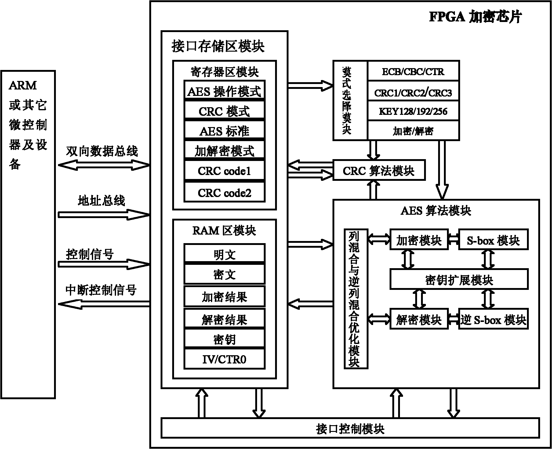
[0071] Secondly, describe the overall structure of the AES encryption chip, see figure 2 shown.

[0072] The hardware architecture design is based on ARM or other microcontrollers and devices as the main controller, and the FPGA encryption chip as the coprocessor, such as figure 2 shown. The main controller completes the management work of the entire encryption system, involving encryption or decryption mode setting, operation mode setting, initial key, initial vector IV (CBC mode) and initial count value CTR0 (CTR mode) setting and CRC (Cyclic Redundancy Check) mode settings. After setting these modes, the FPGA works according to the corresponding requirements.

[0073] The AES encryption c...


PUM


Abstract

The invention discloses a method for designing an AES (Advanced Encryption Standard) encryption chip based on an FPGA (Field Programmable Gate Array), which is designed for aiming at the requirement of an embedded system. The AES encryption chip not only can be used in a manner of a solid chip but also used in a manner of a software module. Three operation modes of ECB (Electronic Code Book), CBC (Cipher Block Chaining) and CTR (Counter Technical Requirement) are supported simultaneously. All standards of the AES can be encrypted and decrypted. The byte replacement and the key expansion are carried out by using a look-up table optimization algorithm. A column mixed optimization structure is provided. Device resources are saved while the operation speed is ensured. An RAM (Random-Access Memory) can be configured as a cache of information and a key through double ports of the FPGA. A problem for storing a time sequence and data of other devices or equipment and the FPGA is resolved. Safe and reliable communication with an FPGA interface joins CRC (Cyclic Redundancy Check) error detection in a manner of a memory bus. The AES encryption chip has the advantages of high safety, high encryption and decryption speeds, low device resource requirement, low cost and the like. The AES encryption chip can be widely used in information technology industries of intelligent card systems, ATMs (Automatic Teller Machines), wireless local area networks, wireless sensor networks and the like.

Description

technical field [0001] The invention relates to an IC chip and an embedded encryption system design method for encrypting and decrypting information and data. That is, it makes full use of the hardware reliability of FPGA and the flexibility of logic programming to realize the AES encryption algorithm, which also involves the design method of how to reduce device resources while ensuring the processing speed. This method supports all AES standards and three non- Feedback mode: electronic code book (ECB), cipher block chaining mode (CBC) and counter mode (CTR), and how this chip is applied to embedded systems. Background technique [0002] At present, the information technology industry at home and abroad needs encryption and decryption systems to improve information security, such as smart card systems (Smart Card), mobile banking systems (Cell Phone Bank), World Wide Web (WWW), ATM cash machines, wireless local area networks (WLAN), Wireless Sensor Network (WSN), etc. [...

Claims


Application Information

Patent Timeline
IPC IPC(8): H04L9/06
Inventor 朱敏玲王曦覃道亮赵威力吉思环甘新鹏
Owner BEIHANG UNIV
Why Eureka
Try Eureka