Press-pack module with power overlay interconnection

一种电力、封装件的技术,应用在压装半导体模块领域

Active Publication Date: 2011-11-09
GENERAL ELECTRIC RENOVABLES ESPANA SL
View PDF4 Cites 19 Cited by
  • Summary
  • Abstract
  • Description
  • Claims
  • Application Information

AI Technical Summary

Problems solved by technology

However, in the complex design of commercial semiconductor packages, and with the small size of existing semiconductor chips, typical springs may not be sufficient for accurate alignment with the semiconductor chips in the package

Method used


Image

  • Press-pack module with power overlay interconnection
  • Press-pack module with power overlay interconnection
  • Press-pack module with power overlay interconnection

Examples


Embodiment Construction

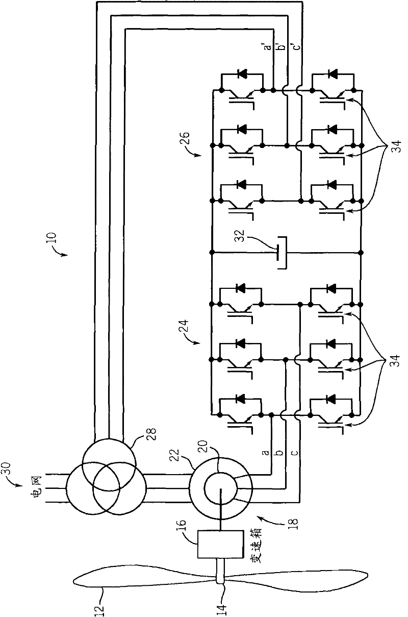
[0019] Turning to the attached picture, figure 1 A wind power converter system 10 is depicted that may include press-packed semiconductor modules in accordance with the present disclosure. The wind power converter system 10 may be adapted to capture energy from wind using turbine blades 12 and convert the captured wind power into mechanical power and convert the mechanical power into electrical power. The system 10 may include a gearbox 16 coupled to a turbine rotor 14 of the turbine blades 12 . The gearbox 16 may accommodate the relatively low speed of the turbine rotor 14 with the relatively high speed of the generator 18 .

[0020] The generator 18 may convert mechanical power to electricity and may be, for example, an induction generator or a synchronous generator. For example, in figure 1 The generator 18 illustrated in FIG. 2 may be a doubly-fed induction generator (DFIG), which includes rotor windings 20 and stator windings 22 . The stator windings 22 of the generat...


PUM


Abstract

Systems and methods for utilizing power overlay (POL) technology and semiconductor press-pack technology to produce semiconductor packages (50, 70, 78, 80, 90, 100, 110, 120) with higher reliability and power density are provided. A POL structure (40) may interconnect semiconductor devices (48) within a semiconductor package (50, 70, 78, 80, 90, 100, 110, 120), and certain embodiments may be implemented to reduce the probability of damaging the semiconductor devices (48) during the pressing of the conductive plates (58, 60). In one embodiment, springs (54) and / or spacers (56) may be used to reduce or control the force applied by an emitter plate (58) onto the semiconductor devices (48) in the package (50, 70, 78, 80, 90, 100, 110, 120). In another embodiment, the emitter plate (58) may be recessed to exert force on the POL structure (40), rather than directly against the semiconductor devices (48). Further, in some embodiments, the conductive layer (42) of the POL structure (40) may be grown to function as an emitter plate (58), and regions of the conductive layer (40) may be made porous to provide compliance.

Description

technical field [0001] The subject matter disclosed herein relates to electronic devices, and more particularly to press-packed semiconductor modules using electrical overlay interconnects. Background technique [0002] In various power electronic systems, press-packed semiconductor packages can be used to control the distribution of power to various applications and devices of the power electronic system. A press-pack semiconductor package may generally include a number of semiconductor chips that function as current switches for relatively high voltage ranges. The semiconductors used in this package have certain limitations, such as maximum breakdown voltage and current carrying capability. Due to the blocking voltage limitation of each individual semiconductor, several semiconductors can be connected in series to obtain the required voltage and function in higher power systems. For example, insulated gate bipolar transistors (IGBTs) may have a relatively low breakdown v...

Claims


Application Information

Patent Timeline
Patent Type & Authority Applications(China)
IPC IPC(8): H01L25/00H01L25/07H01L23/31H01L23/00H01L23/48
CPCH01L2924/01013H01L2924/01082H01L2924/01033H01L23/48H01L2924/01049H01L2924/0103H01L2924/10329H01L25/072H01L2924/13055H01L2924/30105H01L25/071H01L2224/18H01L2924/19041H01L24/72H01L2924/01029H01L2924/01006H01L2924/01078H01L24/82H01L2924/01042H01L24/24H01L2924/13091H01L2224/24137H01L2224/73267H01L2924/1306H01L2924/1301H01L2924/13034H01L2924/1305H01L2924/351H01L2924/10253H01L2924/10272H01L2924/1033H01L2924/1302H02P2101/15H01L2224/04105H01L2224/0603H01L2924/00H01L2924/00014
Inventor A·V·高达A·埃拉泽尔S·S·甘图里
Owner GENERAL ELECTRIC RENOVABLES ESPANA SL
Why Eureka
Try Eureka