Mixed multispectral photosensitive pixel group, photosensitive device and photosensitive system

A photosensitive device and pixel group technology, applied in the photosensitive field, can solve the problems of limited photosensitive efficiency of chemically coated photosensitive devices

Active Publication Date: 2011-11-16
BOLYMEDIA HLDG
View PDF7 Cites 6 Cited by
  • Summary
  • Abstract
  • Description
  • Claims
  • Application Information

AI Technical Summary

Problems solved by technology

With this invention, a filter film and an additional semiconductor reading layer are required, and the use of a filter film limits the photosensitive efficiency of the chemically coated photosensitive device

Method used


Image

  • Mixed multispectral photosensitive pixel group, photosensitive device and photosensitive system
  • Mixed multispectral photosensitive pixel group, photosensitive device and photosensitive system
  • Mixed multispectral photosensitive pixel group, photosensitive device and photosensitive system

Examples


Embodiment Construction

[0091] The present invention will be further described in detail below through specific embodiments in conjunction with the accompanying drawings.

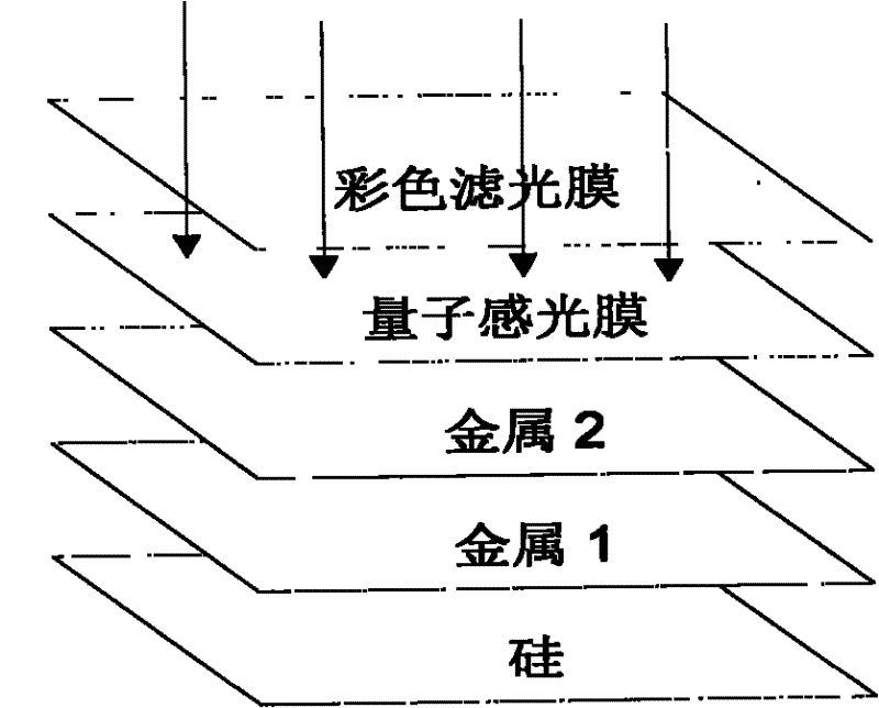
[0092] The invention relates to the design, manufacture and system use of a photosensitive device, especially a multi-spectrum photosensitive device with large array and high performance. The present invention integrates novel quantum dot photosensitive film or other possible coating photosensitive pixel technology and mature semiconductor photosensitive chip technology, and invents a new hybrid photosensitive device and its system, which combines semiconductor (CCD or CMOS) photosensitive device And the advantages of electroless coating (such as quantum film) photosensitive devices, in order to obtain multi-spectrum photosensitive devices that reach or approach the theoretical limit of light use efficiency.

[0093] In the embodiment of the present invention, firstly, a mixed multi-spectral photosensitive pixel group is provided,...


PUM


Abstract

The invention relates to a mixed multispectral photosensitive pixel group, a photosensitive device and a photosensitive system. The mixed multispectral photosensitive pixel group comprises at least one photosensitive pixel of chemical coating and at least one photosensitive pixel of semiconductor. In the invention, the photosensitive pixel of chemical coating is combined with the photosensitive pixel of semiconductor to generate the mixed multispectral photosensitive pixel so that a plurality of color signals and other spectrum signals can be simultaneously obtained, incident photon energy can be maximally used and an upper bound of a photoelectric conversion efficiency theory can be or almost be reached. Images of other spectrums, such as an ultraviolet image, a near infrared image and a far-infrared image, can be acquired and simultaneously colors can be completely reconstructed.

Description

technical field [0001] The invention relates to the photosensitive field, in particular to a mixed multi-spectrum photosensitive pixel group, a photosensitive device, and a photosensitive system. Background technique [0002] The present invention is based on "Multi-spectral photosensitive device and its manufacturing method" (PCT / CN2007 / 071262), "Multi-spectral photosensitive device and its manufacturing method" (Chinese application number: 200810217270.2) and "Multi-spectral photosensitive device" (PCT / CN2007 / 071262) earlier by the inventor. Device" (Chinese application number: 200910105372.X), "A multi-spectral photosensitive device and its sampling method" (Chinese application number: 200910105948.2), "A photosensitive device and its reading method, reading circuit" (Chinese application No.: 200910106477.7) is a continuation, aiming to provide a more specific and optimal chip and system-level implementation. [0003] The inventions listed above mainly relate to the manu...

Claims


Application Information

Patent Timeline
Patent Type & Authority Applications(China)
IPC IPC(8): H01L27/146H04N5/335
Inventor 胡笑平
Owner BOLYMEDIA HLDG
Why Eureka
Try Eureka