Cs-activation-free heterojunction type GaN negative electron affinity photoelectric cathode

A technology of photocathode and negative electrons, which is applied in the direction of electron multiplier cathode devices, multiplier electrodes, detailed information of electron multipliers, etc. It can solve the problems of shortening the service life of the device, the decrease of cathode sensitivity, and the difficulty of accurately controlling the Cs flow, etc., to achieve extended The effect of service life and difficulty reduction

Active Publication Date: 2011-11-23
NO 55 INST CHINA ELECTRONIC SCI & TECHNOLOGYGROUP CO LTD
View PDF3 Cites 6 Cited by
  • Summary
  • Abstract
  • Description
  • Claims
  • Application Information

AI Technical Summary

Problems solved by technology

However, it is difficult to precisely control the flow of Cs during the fabrication of traditional NEA cathodes, which increases the difficulty of making high-quality NEA cathodes.
In addition, the chemical activity of Cs is very high, and it is very easy to react with other substances, so the cathode after Cs activation needs to be maintained in an ultra-high vacuum

Method used


Image

  • Cs-activation-free heterojunction type GaN negative electron affinity photoelectric cathode
  • Cs-activation-free heterojunction type GaN negative electron affinity photoelectric cathode
  • Cs-activation-free heterojunction type GaN negative electron affinity photoelectric cathode

Examples


Embodiment Construction

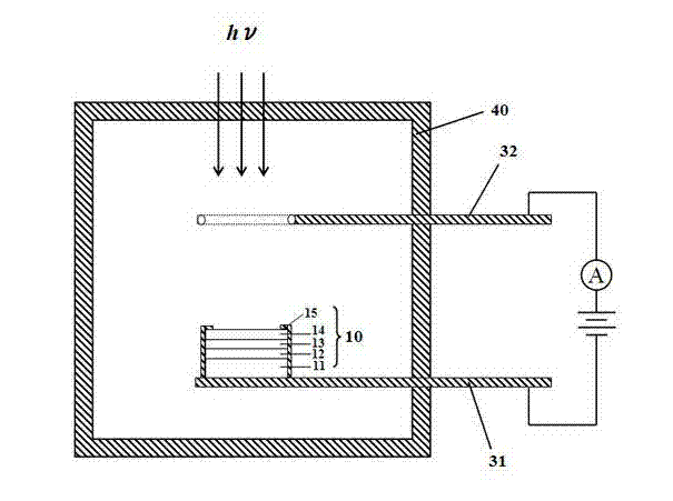
[0020] Below in conjunction with accompanying drawing and specific embodiment, further illustrate the present invention, should be understood that these embodiments are only for illustrating the present invention and are not intended to limit the scope of the present invention, after having read the present invention, those skilled in the art will understand various aspects of the present invention Modifications in equivalent forms all fall within the scope defined by the appended claims of this application.

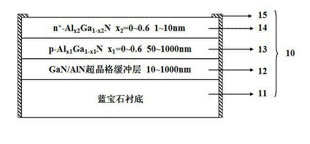
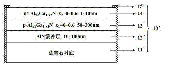
[0021] Such as figure 1 and figure 2 As shown, the structure of a heterojunction GaN negative electron affinity photocathode without Cs activation, including:

[0022] A substrate 11, which is a double-polished sapphire substrate;

[0023] A GaN / AlN superlattice buffer layer 12 or AlN buffer layer 12', the GaN / AlN superlattice buffer layer 12 or AlN buffer layer 12' is grown on a double-thrown sapphire substrate 11, the GaN / AlN superlattice The buffer layer 12 is non...


PUM

PropertyMeasurementUnit
Thicknessaaaaaaaaaa
Thicknessaaaaaaaaaa
Thicknessaaaaaaaaaa

Abstract

The invention discloses a Cs-activation-free heterojunction type GaN negative electron affinity (NEA) photoelectric cathode which comprises a substrate, a GaN/AlN superlattice buffer layer or AlN buffer layer growing on the substrate, a p-Alx1Ga1-x1N light absorption layer growing on the GaN/AlN superlattice buffer layer or AlN buffer layer, an n<+>-Alx2Ga1-x2N cap layer growing on the p-Alx1Ga1-x1N light absorption layer, and electrodes made on the surface edge of the n<+>-Alx2Ga1-x2N cap layer and the side surface of a multilayer material, wherein x1 is more than 0 and less than 1, and X2 is more than 0 and less than 1. According to the invention, an NEA characteristic of a cathode can be achieved without activating Cs, and the advantages of reducing the difficulty of making a high-quality NEA cathode and prolonging the service life of the cathode without maintaining an ultrahigh vacuum environment are achieved.

Description

technical field [0001] The invention belongs to the technical field of semiconductor photoelectric emission, in particular to a heterojunction GaN negative electron affinity photocathode without Cs activation. Background technique [0002] Ultraviolet detection technology has a wide range of applications in the fields of early warning, communication, aerospace, medicine, biology and environmental monitoring. The current ultraviolet detectors mainly include solid-state ultraviolet detectors and vacuum-type ultraviolet photocathode detectors. Solid-state ultraviolet detectors mainly include pn junction type, PIN type, Schottky barrier type and MSM type, which have the advantages of small size, light weight, adjustable detection wavelength, simple working circuit, and no need for high voltage operation. UV-enhanced silicon photodiodes are representative of solid-state UV detectors, but their response to visible light limits their application in the field of UV detection. Wit...

Claims


Application Information

Patent Timeline
IPC IPC(8): H01J43/08
Inventor 唐光华戴丽英钟伟俊姜文海
Owner NO 55 INST CHINA ELECTRONIC SCI & TECHNOLOGYGROUP CO LTD
Why Eureka
Try Eureka