Novel integrated circuit (IC) package manufacturing process

A manufacturing process and process technology, applied in the field of IC packaging technology, can solve the problems of slow packaging speed and poor packaging accuracy, and achieve the effects of rigorous production, improved moisture-proof function, and improved packaging speed

Active Publication Date: 2015-03-18
宁波永旭丰泰电子科技有限公司
View PDF0 Cites 0 Cited by
  • Summary
  • Abstract
  • Description
  • Claims
  • Application Information

AI Technical Summary

Problems solved by technology

[0004] The purpose of the present invention is to provide a new type of IC packaging manufacturing process, which completely replaces the manual packaging process by using special lamination equipment, lamination materials, and segmentation equipment, and solves the problems of poor packaging accuracy and slow packaging speed. technical problems in

Method used


Image

  • Novel integrated circuit (IC) package manufacturing process

Examples


Embodiment Construction

[0055] The present invention is described in further detail below:

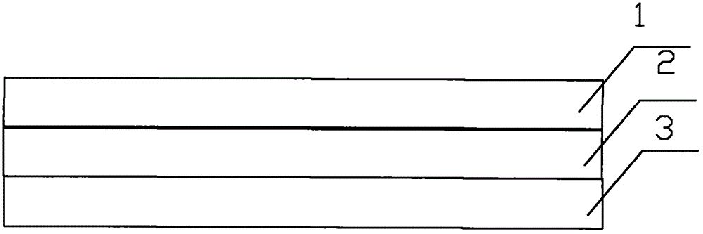
[0056] like figure 1 Shown is the layer structure schematic diagram of the product made by the present invention, and the technological process of production is as follows:

[0057] Step 1, making IC carrier board 3;

[0058] Step 2, preparing the packaging cover plate 2;

[0059] Step 3: Put 50Um resin-type pure glue on the reverse side of the package cover, and press it onto the IC carrier through mechanical integral pressing; in this pressing step, the temperature needs to be controlled at 170-180 degrees, and the time should be controlled within 30 minutes.

[0060] Step 4, use ±0.05mm high-precision engraving machine to engrave and shape,

[0061] Step 5, bind the IC carrier board 3 through the binding machine,

[0062] Step 6, cover the front of the packaging cover plate 2 with 50Um resin type pure glue,

[0063] In step 7, the encapsulation glass 1 is mechanically laminated on the encapsulation co...


PUM


Abstract

The invention discloses a novel integrated circuit (IC) package manufacturing process, which comprises the following steps of: manufacturing an IC carrier plate; preparing a packaging cover plate; gluing a reverse side of the packaging cover plate, and wholly pressing the reverse side of the packaging cover plate on the IC carrier plate mechanically; and carving and molding by adopting a + / -0.05mm high-precision carving machine, binding the IC carrier plate by using a binding machine, coating 50Um resin pure glue on a positive side of the packaging cover plate, wholly pressing packaging glass on the cover plate mechanically, and cutting and molding by using a cutting machine. The process has the advantages that: various parts are wholly pressed by resin pure glue, the traditional manual monomer package is replaced, and the packaging speed is greatly improved; the packaging cover plate is molded through high-precision computerized numerical control (CNC), a monomer plastic piece injection molding mode is replaced, and the packaging precision is improved; the wholly pressed products are cut by a wafer cutting machine, and the packaging precision is improved; and various parts are wholly pressed by the resin pure glue, the density among the various parts is improved, and the moistureproof function after package is improved.

Description

technical field [0001] The invention relates to an IC packaging technology, in particular to a novel IC packaging technology. Background technique [0002] IC packaging refers to connecting the circuit pins on the silicon chip to the external joints with wires so as to connect with other devices. The packaging form refers to the shell used to install the semiconductor integrated circuit chip. It not only plays the role of installing, fixing, sealing, protecting the chip and enhancing the electrothermal performance, but also connects the contacts on the chip to the pins of the package shell with wires, and these pins pass through the wires on the printed circuit board. Connect with other devices to realize the connection between the internal chip and the external circuit. Because the chip must be isolated from the outside world to prevent impurities in the air from corroding the chip circuit and causing electrical performance degradation. [0003] At present, similar IC pac...

Claims


Application Information

Patent Timeline
Patent Type & Authority Patents(China)
IPC IPC(8): H01L21/56H01L21/48
Inventor 陈胜华
Owner 宁波永旭丰泰电子科技有限公司
Why Eureka
Try Eureka