Shallow slot negative bevel terminal structure and preparation method thereof

A terminal structure and bevel technology, applied in semiconductor/solid-state device manufacturing, electrical components, circuits, etc., can solve the problems of large chip area and poor stability, and achieve the effect of reducing process cost and taking into account stability and mechanical strength.

Active Publication Date: 2011-11-23
XIAN SEMIPOWER ELECTRONICS TECH
View PDF1 Cites 8 Cited by
  • Summary
  • Abstract
  • Description
  • Claims
  • Application Information

AI Technical Summary

Problems solved by technology

[0003] The object of the present invention is to provide a shallow groove negative bevel terminal structure suitable for power MOS devices, which solves the problems of poor junction terminal stability and large chip area occupied by existing power MOS devices

Method used


Image

  • Shallow slot negative bevel terminal structure and preparation method thereof
  • Shallow slot negative bevel terminal structure and preparation method thereof
  • Shallow slot negative bevel terminal structure and preparation method thereof

Examples


Embodiment Construction

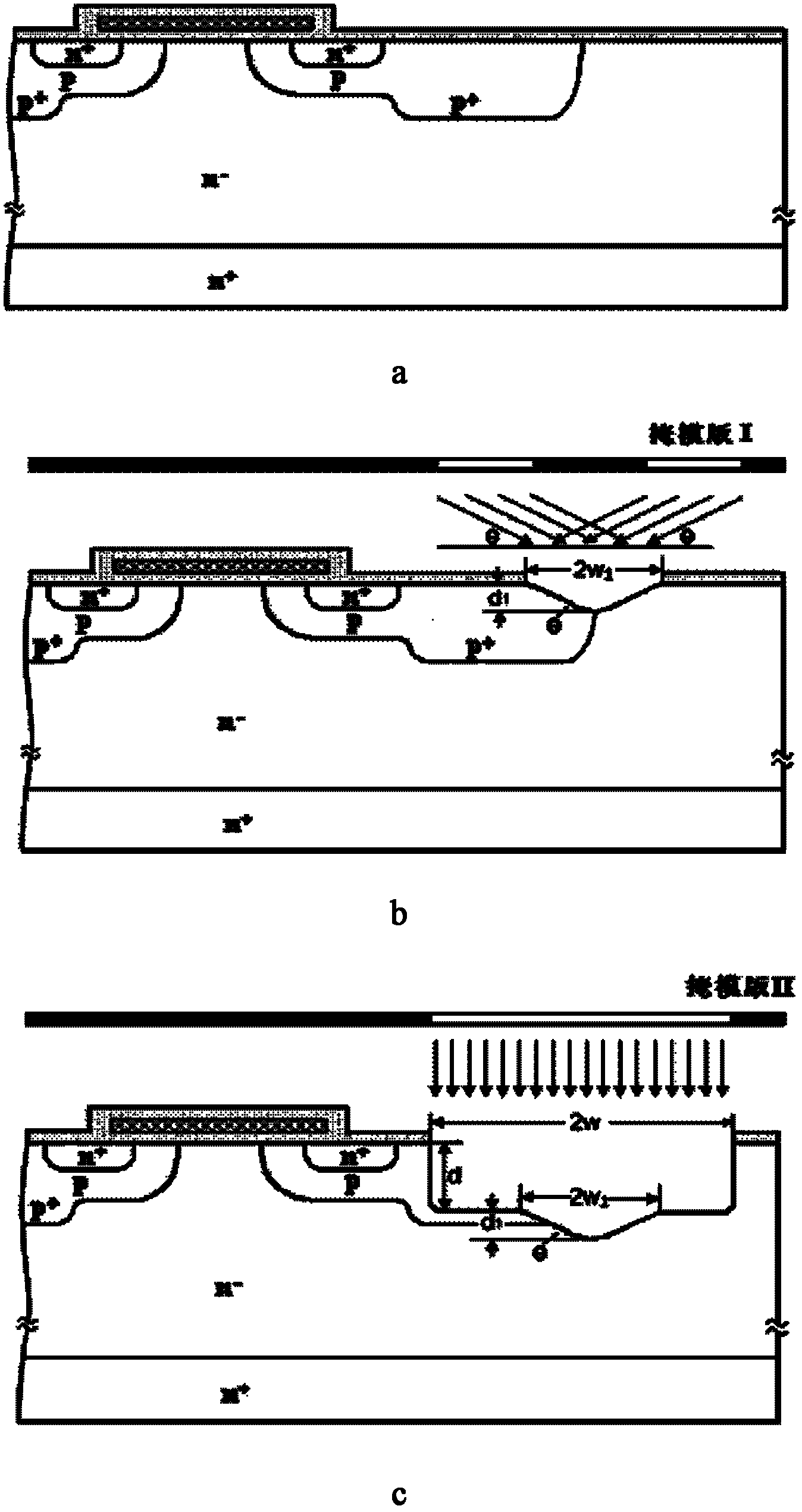
[0017] The present invention will be described in detail below in conjunction with the accompanying drawings and specific embodiments.

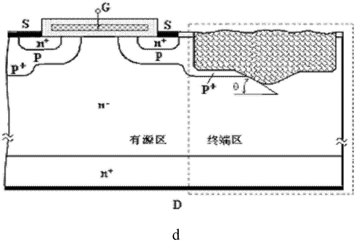
[0018] refer to figure 1 d, the shallow groove negative bevel terminal structure suitable for power MOS devices of the present invention is that the center of the chip is the active area, the periphery is the terminal area, and the common n of the active area and the terminal area + The bottom of the substrate is the drain D of the device, n + n - drift zone;

[0019] n in the active area - There are multiple cells in the drift area, and the bottom of each cell is p + well area, p + Above the well region is the p-body region, and the n-body region is set in the p-body region. + source area, n + Above the source region is the source electrode S, and the source electrode S will be n + The source region is short-circuited to the p-body region; a polysilicon gate G is provided between two adjacent source electrodes S, and a gate oxide lay...


PUM


Abstract

The invention discloses a shallow slot negative bevel terminal structure applicable to a power metal oxide semiconductor (MOS) device, and a preparation method thereof. An active region is formed in the center of a chip and a terminal region is formed at the periphery of the chip; the bottom of an n+ substrate shared by the active region and the terminal region is provided with a drain of the device; an n- drift region is formed on the n+ substrate; a plurality of cells are arranged in the n- drift region of the active region; a p+ well region is formed on the lowermost part of each cell; a pbody region is formed on the p+ well region; an n+ source region is formed in the p body region; a source electrode is arranged on the n+ source region; the n+ source region is in short circuit connection with the p body region through the source electrode; a polysilicon gate is arranged between two adjacent source electrodes; a gate oxide layer is arranged under the polysilicon gate; and in the p+ well region of the terminal region, a slot of which the two sides are vertical and the bottom extends into the n- drift region is formed by a two-step etching method, and silicon oxynitride is filled in the whole slot. By the structure, breakdown voltage, terminal area, stability and mechanical strength are considered.

Description

technical field [0001] The invention belongs to the technical field of power semiconductor devices, and relates to a shallow groove negative bevel terminal structure suitable for power MOS devices, and also relates to a preparation method of the shallow groove negative bevel terminal structure. Background technique [0002] In the manufacturing process of power MOS high-voltage devices, the choice of terminal technology will directly affect its withstand voltage and its stability. Commonly used junction termination technologies are field plate (FP), field limiting ring (FLR), junction termination extension (JTE), variable lateral doping (VLD), mesa technology and its composite technology. Since power MOS devices (such as power MOSFETs and IGBTs) adopt a multi-cell parallel structure, the pn junction end of the outermost cell is terminated on the surface, and its p-region is relatively shallow. Therefore, conventional mechanical angle grinding methods cannot be used. To form...

Claims


Application Information

Patent Timeline
Patent Type & Authority Applications(China)
IPC IPC(8): H01L29/06H01L29/78H01L21/336
CPCH01L29/7811H01L29/0661H01L29/66712
Inventor 王彩琳于凯
Owner XIAN SEMIPOWER ELECTRONICS TECH
Why Eureka
Try Eureka