A device and method for double-sided alignment of an inner layer board

A technology of alignment device and inner layer board, which is applied to the exposure device of photoengraving process, the removal of conductive materials by chemical/electrolytic methods, and the photoengraving process of pattern surface, etc. holes, etc., to simplify the production process, the method is simple, and the alignment accuracy is improved.

Inactive Publication Date: 2011-11-30
HEFEI ADVANTOOLS SEMICON
View PDF5 Cites 27 Cited by
  • Summary
  • Abstract
  • Description
  • Claims
  • Application Information

AI Technical Summary

Problems solved by technology

[0004] The purpose of the present invention is to provide a device and method for aligning both sides of the inner layer board, which only needs to install a set of image acquisition device under the object table, so as to solve the problem of punching holes in the inner layer of the circuit board in the prior art. And increase the problem of UV-Marker device

Method used


Image

  • A device and method for double-sided alignment of an inner layer board
  • A device and method for double-sided alignment of an inner layer board
  • A device and method for double-sided alignment of an inner layer board

Examples


Embodiment Construction

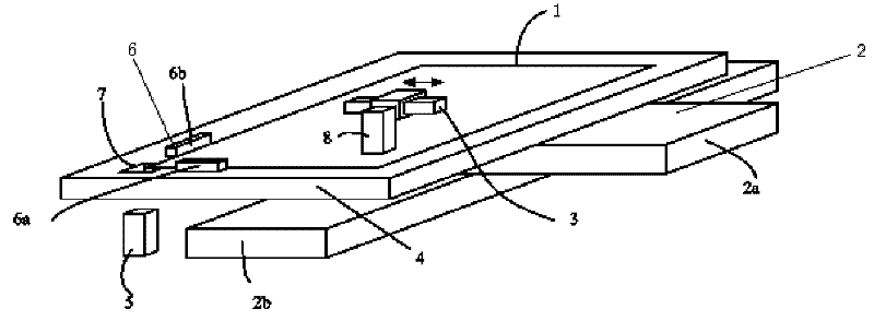
[0029] Such as figure 1 As shown, the alignment device for both sides of the inner plate of the present invention includes: a stage 4, a coarse positioning device 6 composed of a left positioning bar 6a and a lower side positioning bar 6b, and a kinematic pair 2a in the X direction and a Y direction The precision X-Y mobile platform 2 that the motion pair 2b constitutes, the lower image acquisition device 5, the upper image acquisition device 8, the one-dimensional mobile platform 3, the detection through hole 7, the control processing unit ( figure 1 not shown).

[0030] The stage 4 is used to place the circuit board 1 to be exposed, and the circuit board 1 is tightly attached to the stage 4 by vacuum adsorption.

[0031] The positioning bars 6a, 6b are perpendicular to each other and are on the same plane, and are installed on the stage 4 for positioning the circuit board 1 .

[0032] The precision X-Y moving platform 2 is used to move the circuit board 1 to a designated p...


PUM


Abstract

The invention discloses a double-side aligning device and method for an inner plate, which is suitable for a laser direct imaging system (LDI). In order to reduce the time required for alignment, at least two sets of image acquisition devices are used to simultaneously measure the alignment marks, one of which is installed above the stage, and the other image acquisition device is installed below the stage. In order to meet the requirements of fast alignment of inner boards of different sizes, one image acquisition device is fixed, and the other image acquisition device is installed on a single-axis moving mobile platform. Using the method of image processing, the feature points at the corners of the inner board are extracted for double-sided alignment.

Description

technical field [0001] The invention relates to the fields of circuit board manufacturing and image processing, in particular to a device and method for double-sided alignment of an inner layer board applied to a laser direct imaging system. Background technique [0002] Laser direct imaging technology (Laser direct imaging, LDI) is to use the data output by the CAM workstation to directly drive the laser direct imaging device, and perform image imaging on the circuit board substrate coated with photoresist (similar to laser photopainting). machine on the polyester base sheet for graphic imaging), and then develop to get the desired graphics, and then etch, remove the film (remove the remaining photoresist), then get the desired pattern on the circuit board Copper conductor graphics up. Obviously, LDI not only reduces many processes such as negative film manufacturing, application, storage and maintenance, and simplifies the process, but more importantly, eliminates the PCB...

Claims


Application Information

Patent Timeline
Patent Type & Authority Applications(China)
IPC IPC(8): G03F7/20G03F9/00H05K3/06
Inventor 徐玉华何少锋蒋兴华
Owner HEFEI ADVANTOOLS SEMICON
Why Eureka
Try Eureka