

short circuit thyristor
A technology of thyristor and conduction type, which is applied in the field of short-circuit thyristors, and can solve the problems of reducing the turning voltage, the influence and difficulties of the characteristics of thyristor holding current, etc.
- Summary
- Abstract
- Description
- Claims
- Application Information
AI Technical Summary
Problems solved by technology
Method used
Image

Examples
Embodiment approach 1
[0027] Hereinafter, a short-circuit thyristor according to Embodiment 1 of the present invention will be described with reference to the drawings.
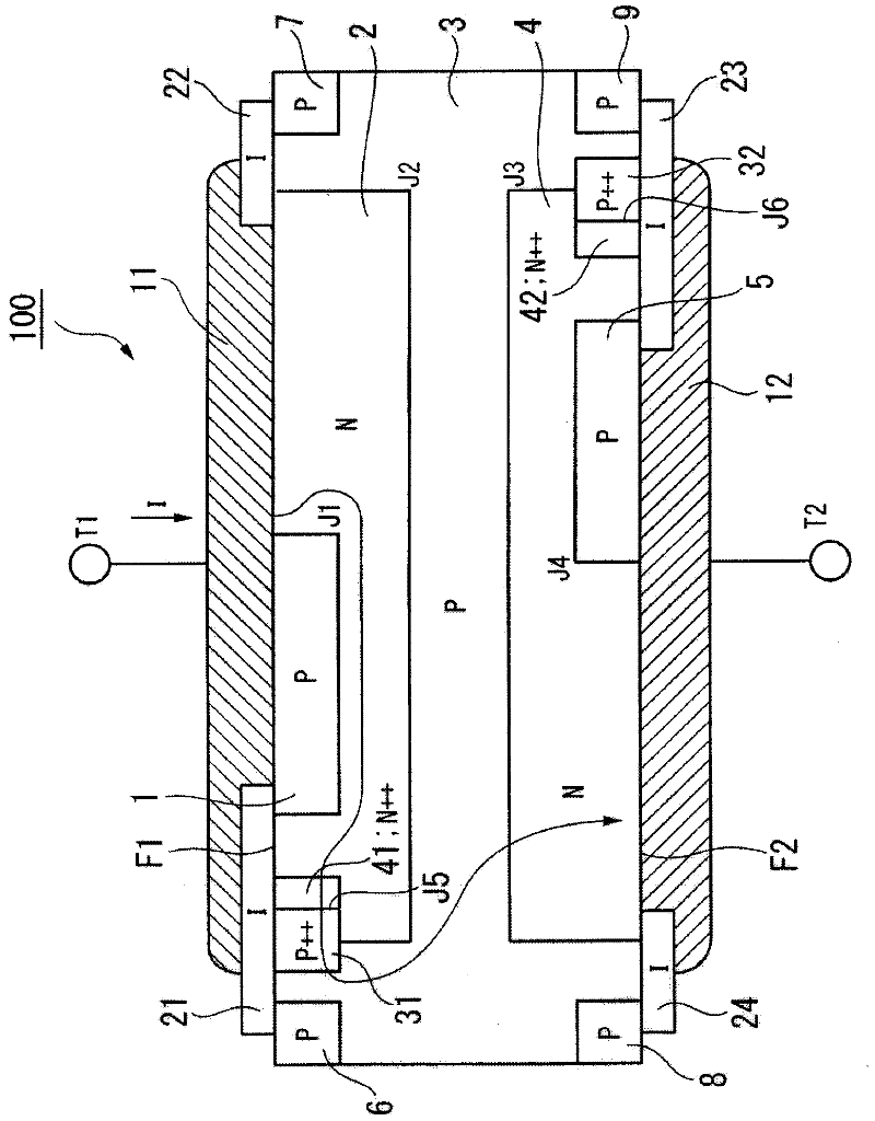
[0028] figure 1 It is a cross-sectional structural view showing the short-circuited thyristor 100 according to the first embodiment.
[0029] exist figure 1 Among them, the short-circuit thyristor 100 has a P region (1, 3, 5), an N region (2, 4), a channel stopper (channel stopper) (6-9), electrodes (11, 12), an insulating layer (21-24), P++ area (31, 32), and N++ area (41, 42).
[0030] The P region 3 is a p-type semiconductor region of the first conductivity type and constitutes a semiconductor substrate of the main body layer of the short-circuit thyristor 100 . Here, will figure 1 The upper side of the semiconductor substrate is the first surface F1, and the lower side of the semiconductor substrate is the second surface F2.
[0031] The N region 2 is an n-type semiconductor region of the second conductivity type. N r...
Embodiment approach 2
[0062] Next, a short-circuit thyristor according to Embodiment 2 of the present invention will be described with reference to the drawings.
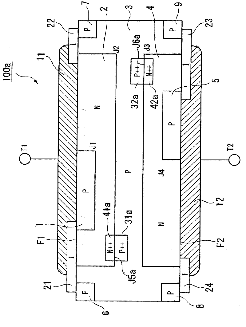
[0063] figure 2 It is a cross-sectional structural view showing a short-circuited thyristor 100a according to the second embodiment.
[0064] exist figure 2 Among them, the short-circuit thyristor 100a has P regions (1, 3, 5), N regions (2, 4), channel stop rings (6-9), electrodes (11, 12), insulating layers (21-24 ), P++ regions (31a, 32a), and N++ regions (41a, 42a). exist figure 2 in, for with figure 1 Identical structures are marked with the same symbols.
[0065] The P++ region 31 a is formed in contact with the P region 3 under the insulating layer 21 and is a p-type semiconductor region having a higher impurity concentration than the P region 3 . In addition, the P++ region 31 a is formed in the portion of the junction J2 below the P region 1 .
[0066]The P++ region 32 a is formed in contact with the P region 3 above t...
Embodiment approach 3
[0084] Hereinafter, a three-short-circuit thyristor according to an embodiment of the present invention will be described with reference to the accompanying drawings.
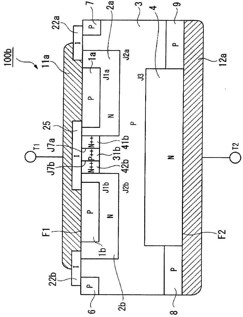
[0085] image 3 It is a cross-sectional structure diagram showing the short-circuited thyristor 100b of the third embodiment.
[0086] exist image 3 Among them, the short-circuit thyristor 100b has P regions (1a, 1b, 3), N regions (2a, 2b, 4), channel stop rings (6-9), electrodes (11a, 12a), insulating layers (22a , 22b, 25), P++ region 31b, and N++ region (41b, 42b). exist image 3 in, for with figure 1 Identical structures are marked with the same symbols.
[0087] The P regions 1a and 1b are p-type semiconductor regions and are formed in a state exposed on the first surface F1.
[0088] N region 2 a is an n-type semiconductor region and is formed between P region 1 a and P region 3 . In addition, a part of the N region 2a is in contact with the first surface F1.
[0089] N region 2 b is an n-type s...
PUM
 Abstract
Description
Claims
Application Information