

Wafer-level packaging structure and method of forming the same
A wafer-level packaging and chip mounting technology, which is applied in radiation control devices, electrical components, and electrical solid-state devices, etc., and can solve the problems of high wafer-level packaging process requirements, complex wafer-level packaging processes, and large restrictions on the size of chips. problem, to achieve the effect of high packaging quality, simple structure, and large room for manoeuvre
- Summary
- Abstract
- Description
- Claims
- Application Information
AI Technical Summary
Problems solved by technology
Method used
Image

Examples
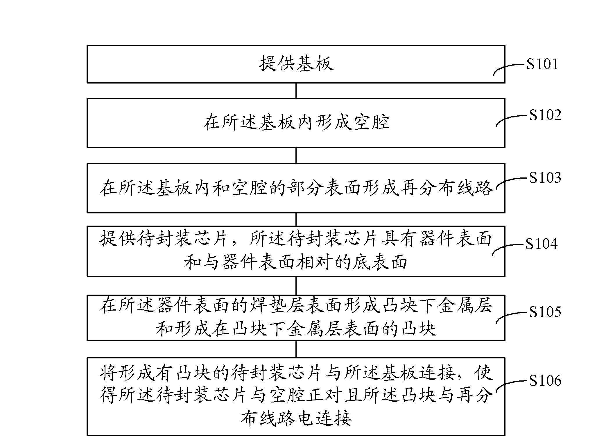
no. 1 example
[0063] The method for forming the wafer-level packaging structure of the present invention will be described in detail below in conjunction with the first embodiment, please refer to image 3 , including the following steps:
[0064] Step S201, providing a first substrate, the first substrate has an opening, and the surface of the substrate facing away from the opening has an infrared filter film;
[0065] Step S202, providing a second substrate, the second substrate has a first surface and a second surface opposite to the first surface;
[0066] Step S203, bonding the surface of the first substrate with the opening to the first surface of the second substrate;
[0067] Step S204, forming a redistribution line on the second surface of the second substrate, the redistribution line exposes part of the second surface, and the exposed second surface corresponds to the position of the opening;
[0068] Step S205, forming a protective layer on the surface of the redistribution lin...
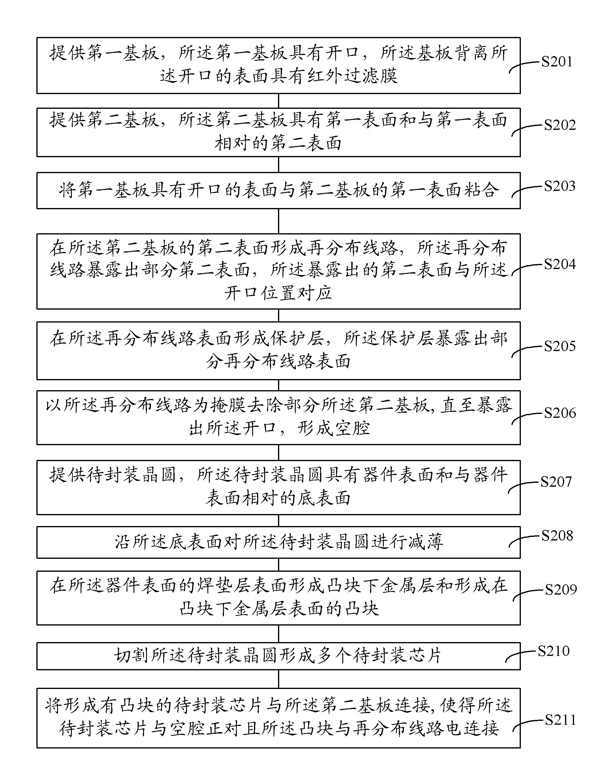
no. 2 example
[0118] The method for forming the wafer-level packaging structure of the present invention will be described in detail below in conjunction with the second embodiment, please refer to Figure 16 , including the following steps:
[0119] Step S301, providing a first substrate, the first substrate has a first opening, and the surface of the first substrate facing away from the first opening has an infrared filter film;
[0120] Step S302, providing a second substrate, the second substrate has a first surface and a second surface opposite to the first surface;
[0121] Step S303, bonding the surface of the first substrate having the first opening to the first surface of the second substrate;
[0122] Step S304, removing part of the second substrate along the second surface until the first substrate is exposed to form a second opening, the second opening completely exposes the first opening, and the width of the second opening is greater than the width of the first opening;
[0...
no. 3 example
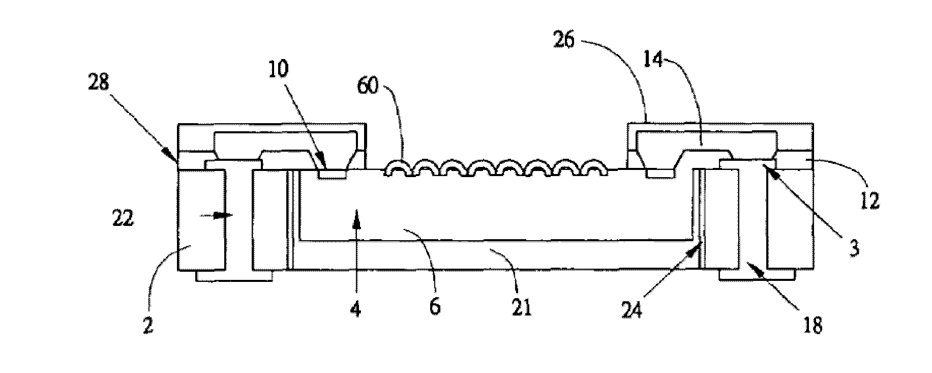
[0147] Please refer to Figure 23 The difference between the wafer-level packaging structure forming method of this embodiment and the second embodiment is that: the first opening 301 and the second opening 304 are located in the second substrate 310, and the width of the second opening 304 is larger than that of the first opening 301 For the subsequent formation process, reference may be made to the corresponding steps in the second embodiment.
[0148] The wafer-level packaging structure formed by this embodiment includes: a first substrate 300, an infrared filter film 302 located on the surface of the first substrate 300; a second substrate 310 located on the surface of the first substrate 300 facing away from the infrared filter film 302; In the second substrate 310 and through the first opening 301 and the second opening 304 of the second substrate 310, and the width of the second opening 304 is greater than the width of the first opening 301; formed on the surface of the...
PUM
 Abstract
Description
Claims
Application Information