Gasket for manufacturing touch panel, method of manufacturing touch panel using the same, and touch panel manufactured by the method

A touch panel and pad technology, applied in the input/output process of data processing, instruments, electrical digital data processing, etc., can solve the problems of residual bubbles, difficulty in manufacturing high-resolution touch panels, etc. The effect of omitting the high-temperature curing process and annealing process and increasing the margins

Inactive Publication Date: 2011-12-14
SHINWA ELECTRONICS IND
View PDF4 Cites 6 Cited by
  • Summary
  • Abstract
  • Description
  • Claims
  • Application Information

AI Technical Summary

Problems solved by technology

Therefore, there is a problem that air bubbles remain in the process of bonding the adhesive layer and the window portion, and defects are likely to occur. Since the overall height of the touch panel becomes high, it is difficult to manufacture a thin device.
[0005] In addition, when forming electrodes, since silver paste is used, there is a limitation in forming fine electrode patterns, making it difficult to manufacture high-resolution touch panels.

Method used


Image

  • Gasket for manufacturing touch panel, method of manufacturing touch panel using the same, and touch panel manufactured by the method
  • Gasket for manufacturing touch panel, method of manufacturing touch panel using the same, and touch panel manufactured by the method
  • Gasket for manufacturing touch panel, method of manufacturing touch panel using the same, and touch panel manufactured by the method

Examples


Embodiment Construction

[0022] Hereinafter, the present invention will be described in detail with reference to the drawings.

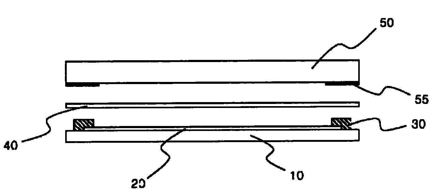
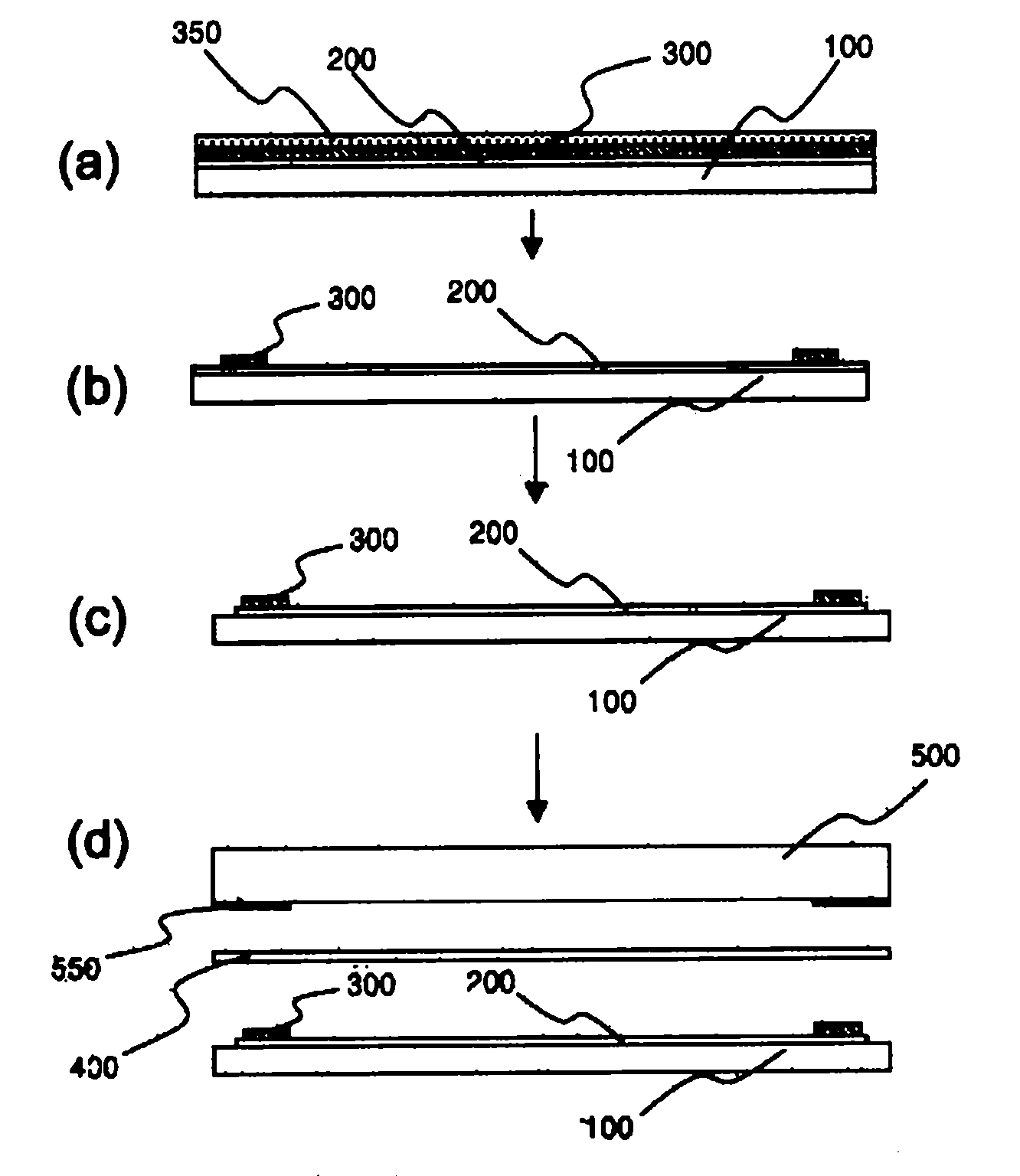
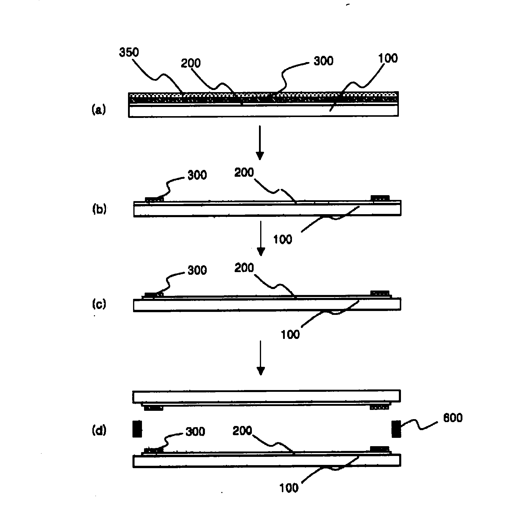
[0023] The present invention relates to a pad for manufacturing a touch panel, which includes: an insulator layer 100 made of an organic insulator or an inorganic insulator; a conductive material coating 200 formed on the upper surface of the insulator layer 100; The metal coating 300 on the upper surface of the conductive substance coating 200 : and the metal protective coating 350 formed on the upper surface of the metal coating.

[0024] A specific example of this is Figure 2 to Figure 4 shown. That is, for example, in the case of a conventional touch panel, for example, i) a dielectric film (organic insulator), such as a PET film, in the case of a capacitive method, and ii) a glass (inorganic insulator) in the case of a resistive film method. Insulator), apply a conductive material coating on its upper surface, such as ITO, IZO or ATO, and then provide the material to...


PUM

PropertyMeasurementUnit
thicknessaaaaaaaaaa
thicknessaaaaaaaaaa
thicknessaaaaaaaaaa

Abstract

The present invention relates to a pad for manufacturing a touch panel, a method for manufacturing a touch panel using the pad, and a touch panel manufactured using the method. The pad for manufacturing a touch panel includes: an insulator layer composed of an organic insulator or an inorganic insulator; A conductive material coating on the upper surface of the insulator layer; a metal coating formed on the upper surface of the conductive material coating; and a metal protective coating formed on the upper surface of the metal coating. This has the following effects: it can be produced in a simpler process than the conventional process of applying silver paste, the production is easy, the production cost can be reduced, and a finer wire can be formed, and a small device can be produced, especially in electrostatic In the case of a capacitive touch panel, the height difference can be minimized, and defects such as air bubbles can be prevented from being generated in the bonding surface when the adhesive layer is bonded, and a touch panel with high resolution can be realized, and corrosion of the metal coating can be prevented for a long time. In storage, corrosion can be reduced even after device fabrication, and a reduction in durability life due to corrosion can be prevented.

Description

technical field [0001] The present invention relates to a gasket for manufacturing a touch panel, a method for manufacturing a touch panel using the gasket, and a touch panel manufactured using the method, which can be manufactured in a simpler process than the existing process of applying silver paste, making the manufacturing easier. It is easy, can reduce manufacturing costs, and can form finer wires to make small devices. Especially in the case of electrostatic capacitive touch panels, the height difference can be minimized, and it can prevent the bonding surface from occurring when the adhesive layer is bonded. Defects such as air bubbles can realize a high-resolution touch panel, prevent corrosion of the metal coating and enable long-term storage, and reduce corrosion after the device is manufactured, thereby preventing a decrease in durability due to corrosion. Background technique [0002] In the case of a spacer used to make a general touch panel, it is produced usi...

Claims


Application Information

Patent Timeline
Patent Type & Authority Applications(China)
IPC IPC(8): G06F3/041G06F3/044G06F1/16
CPCG06F3/045G06F3/044G06F2203/04103
Inventor 朴准永郑州铉金世玄裵相模
Owner SHINWA ELECTRONICS IND
Why Eureka
Try Eureka