Method and device for detecting internal defects of optical components

A technology for optical components and internal defects, applied in measuring devices, material analysis through optical means, scientific instruments, etc., can solve the problems of not being able to judge whether the internal defects of optical components meet the requirements, and being unable to distinguish internal defects from surface defects, etc. To achieve the effects of effective detection, suppression of influence, and easy identification

Inactive Publication Date: 2011-12-21
ZHEJIANG NORMAL UNIVERSITY
View PDF3 Cites 24 Cited by
  • Summary
  • Abstract
  • Description
  • Claims
  • Application Information

AI Technical Summary

Problems solved by technology

However, this method still has the following problems: the test result is a two-dimensional distribution, and it is impossible to distinguish internal defects from surface defects, so it is impossible to judge whether the internal defects of the optical element meet the requirements before processing

Method used


Image

  • Method and device for detecting internal defects of optical components
  • Method and device for detecting internal defects of optical components
  • Method and device for detecting internal defects of optical components

Examples


Embodiment Construction

[0030] In the following description, numerous specific details are set forth in order to provide a thorough understanding of the present invention. However, the present invention can be implemented in many other ways different from those described here, and those skilled in the art can make similar extensions without violating the connotation of the present invention, so the present invention is not limited by the specific implementations disclosed below.

[0031] The device for detecting internal defects of optical elements of the present invention will be described in detail below in conjunction with the accompanying drawings.

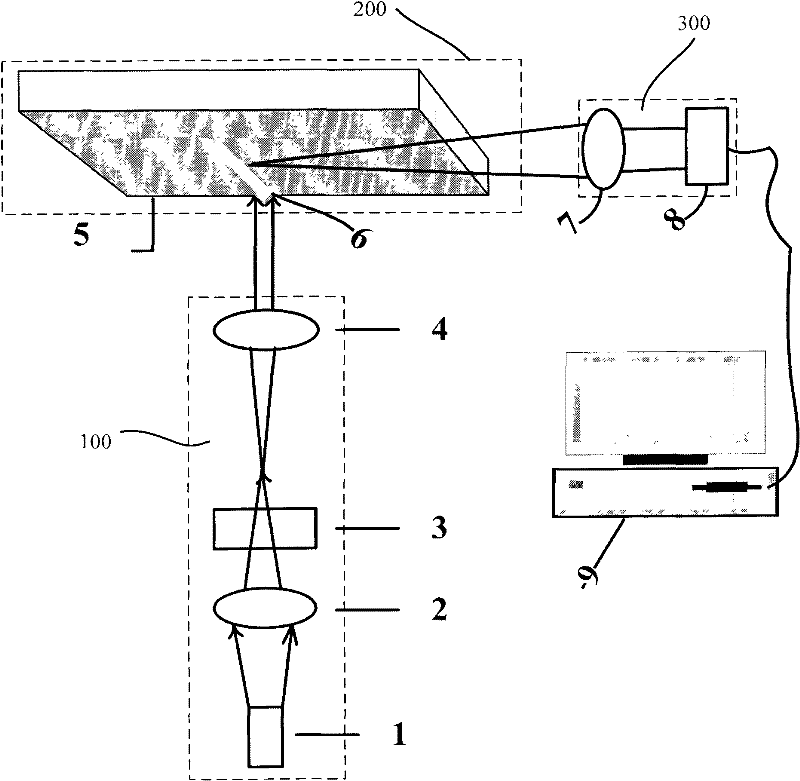
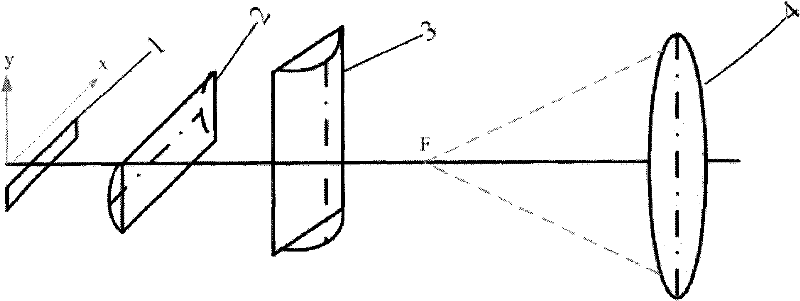
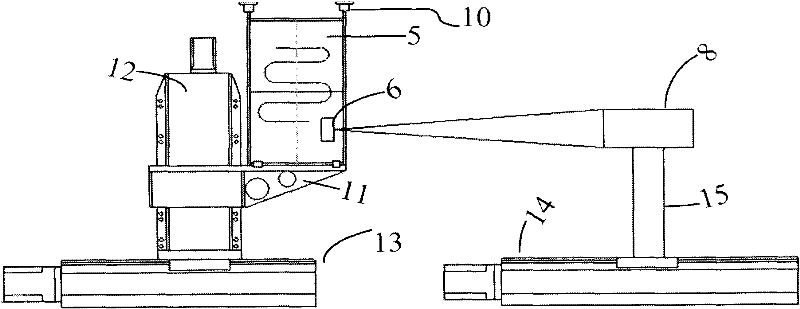
[0032] figure 1 It is a schematic diagram of an embodiment of the detection device for internal defects of optical components of the present invention, please refer to figure 1 , the detection device for internal defects of optical components in this embodiment includes an illumination system 100 , an imaging system 300 and a stage 200 for the compo...


PUM


Abstract

A detection device for internal defects of an optical element, comprising: a stage, an illumination system, and an imaging system; wherein, the position of the illumination system relative to the stage is set in the following manner: when the optical element to be tested is placed on the stage After being mounted, the illumination beam emitted by the illumination system can irradiate the surface of the optical element in a normal incidence mode; the imaging system is arranged outside the side of the optical element on the stage, and can obtain the illumination beam emitted by the illumination system on the optical element. A 2D image of an illuminated section formed in the thickness direction. The device can be used to detect the internal defect of the optical element, and can also distinguish the surface defect from the internal defect. The invention also provides a detection method of the optical element.

Description

technical field [0001] The invention relates to the technical field of optical element detection, in particular to a device and method for detecting internal defects of optical elements made of transparent materials such as glass, plastic, and transparent crystals. Background technique [0002] As a driver for inertial confinement fusion (ICF), a high-power solid-state laser device requires a large number of large-aperture optical elements. However, with the gradual increase in the energy density of high-power solid-state lasers, the ability of optical components to resist laser damage has become a "bottleneck" that hinders the increase in output flux. [0003] Defects in optical components are one of the main factors causing laser damage to optical components. Numerical simulation and experimental results show that the laser damage of optical components is often a local melting crater or bursting at the defect. Because the absorption of laser light by defects in optical c...

Claims


Application Information

Patent Timeline
Patent Type & Authority Applications(China)
IPC IPC(8): G01N21/958
Inventor 徐建程王辉李勇范长江
Owner ZHEJIANG NORMAL UNIVERSITY
Why Eureka
Try Eureka