npn transistor reference voltage generating circuit

A reference voltage and transistor technology, applied in the field of NPN transistor reference voltage generation, can solve the problems of difficult reference voltage, increased system cost, and increased peripheral circuit complexity.

Inactive Publication Date: 2011-12-21
李仲秋
View PDF10 Cites 2 Cited by
  • Summary
  • Abstract
  • Description
  • Claims
  • Application Information

AI Technical Summary

Problems solved by technology

However, only N-type MOS or NPN transistors exist in certain processes. For example, there are only N-type active devices and passive components in the GaAs HBT process for RF power amplifier chips and the GaAs pHEMT process for RF switches ( Including resistors, capacitors and inductors), since there are no P-type devices in these processes, it is difficult to use the traditional bandgap voltage source structure to generate accurate reference voltages. The current solutions provide reference voltages through external circuits, which not only increases The cost of the entire system, but also increases the complexity of peripheral circuits, which is not conducive to system integration and miniaturization

Method used


Image

  • npn transistor reference voltage generating circuit
  • npn transistor reference voltage generating circuit
  • npn transistor reference voltage generating circuit

Examples


Embodiment Construction

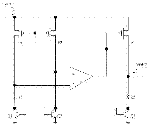
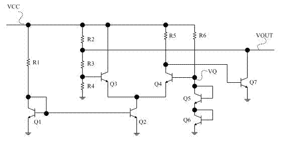
[0005] figure 2 The prototype circuit patented by the present invention consists of 7 NPN transistors and 6 resistors. The base collector of the transistor Q1 is short-circuited and connected to one end of the resistor R1, and the emitter is grounded; one end of the resistor R1 is connected to VCC, and the other end is connected to the transistor. The base collector of Q1; the base of transistor Q2 is connected to the base collector of Q1 and one end of resistor R1, the emitter is grounded, and the collector is connected to the emitters of Q3 and Q4; the two ends of resistor R2 are respectively connected to VCC and VOUT; One end of R3 is connected to VOUT, the other end is connected to the base of Q3 and one end of R4; one end of resistor R4 is connected to the base of Q3 and one end of R3, and the other end is grounded; the base of Q3 is connected to one end of R3 and R4, and the collector is connected to VCC , the emitter is connected to the emitter of Q4 and the collector ...


PUM


Abstract

An NPN transistor reference voltage generating circuit, the technical field of the present invention relates to a method for generating an NPN transistor reference voltage and an NPN transistor reference voltage generating circuit. The present invention provides a reference voltage reference circuit that can be integrated in only N-type active devices and passive component processes, as shown in the figure. The reference voltage is mainly generated in the form of operational amplifier feedback, and the generated reference voltage has good power supply rejection ratio characteristics. The output voltage of this circuit structure has a negative temperature coefficient, which is consistent with the temperature characteristic of the junction voltage drop of the N-type device, which can effectively compensate the change of the junction voltage drop of the N-type device, and obviously improve the temperature characteristic of the circuit. In addition, by adjusting the compensation capacitor, the distribution of the zero and pole points of the loop can be changed, the phase margin of the loop can be improved, and the stability of the loop can be improved.

Description

technical field [0001] The technical field of the patent of the present invention is a method for generating a reference voltage of an NPN transistor, and the present invention also relates to a circuit for generating a reference voltage of an NPN transistor. Background technique [0002] In the traditional complementary metal-oxide-semiconductor (CMOS) process, a bandgap voltage source structure is generally used to generate a reference voltage, such as Figure 1 As shown, this is because in this process, there are all the devices required for the bandgap voltage source circuit, including N-type MOS, P-type MOS, PNP transistors and resistors. The reference voltage (VOUT) generated by this circuit structure It can be expressed as: k*T / q*ln(n)*R2 / R1+Vbe, where k is the Boltzmann constant, T is the temperature, q is the charge, n is the area ratio of Q1 and Q2, and Vbe is The junction voltage drop of the PNP tube can adjust the output value and temperature characteristics of t...

Claims


Application Information

Patent Timeline
Patent Type & Authority Applications(China)
IPC IPC(8): G05F3/20
Inventor 李仲秋
Owner 李仲秋
Why Eureka
Try Eureka