Amorphous thin film transistor and preparation method thereof

An active layer and gate dielectric technology, applied in the direction of transistors, semiconductor devices, electrical components, etc., can solve the problems that cannot meet the requirements of AM-FPD development, and achieve the effect of improving the stability of TFT

Active Publication Date: 2011-12-21
BOE TECH GRP CO LTD
View PDF5 Cites 8 Cited by
  • Summary
  • Abstract
  • Description
  • Claims
  • Application Information

AI Technical Summary

Problems solved by technology

[0008] But the performance of the current MOTFT is only: μ ~ 10cm 2 / (V.s), which is far from meeting the requirements of AM-FPD development

Method used


Image

  • Amorphous thin film transistor and preparation method thereof
  • Amorphous thin film transistor and preparation method thereof
  • Amorphous thin film transistor and preparation method thereof

Examples


Embodiment Construction

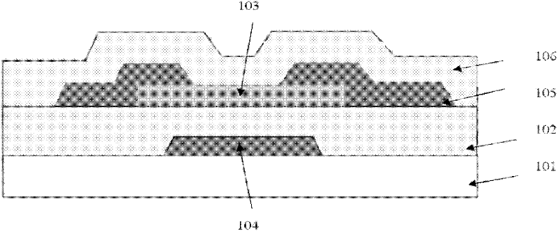
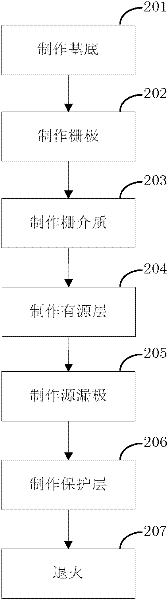
[0015] The present invention will be further described in detail below through specific embodiments in conjunction with the accompanying drawings.

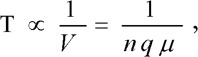
[0016] At present, the main technical problems to be solved by MOTFT are: first, improve the stability of EBS; second, improve the stability of UV light; third, improve μ. The technical solutions for solving the above problems in the embodiments of the present invention include: first, using the active layer with the optimal O content to improve the EBS stability of the MOTFT; second, using the MS process to continuously prepare the amorphous gate dielectric and the active layer process To improve the EBS stability of MOTFT; third, use Mg-doped active layer to improve the UV light stability of MOTFT; fourth, use Ga or Mg-doped In 2 o 3 As the active layer to prepare high μTFT; Fifth, improve the T of the ZnO active layer prepared by MS process S Or use the PLD process to prepare the ZnO active layer to prepare high μZnO TFT.

...


PUM


Abstract

The invention discloses a preparation process of a metal oxide thin film transistor (Metal oxide thin film transistor, MOTFT). First, the active layer with optimal O content is employed to improve the EBS stability of the MOTFT. Second, the Mg-doped active layer is used to improve the UV light stability of the MOTFT. Finally, use rich In2O3 or pure ZnO active layer to improve the mobility of MOTFT.

Description

technical field [0001] The invention relates to a metal oxide thin film transistor (Metal oxide thin film transistor, MOTFT) and a preparation method thereof. Background technique [0002] At present, MOTFT, which has the advantages of low preparation cost, excellent electrical performance and transparency, is very likely to become a new generation of mainstream TFT technology, and will receive a lot of attention in the field of active-matrix flat panel display (AM-FPD). application. However, the disadvantage of MOTFT is that it is easy to absorb or desorb O, H and H 2 O-related molecules, these factors change the electron concentration (N e ) to affect the stability of TFT. The electrical bias stress (EBS) stability of the MOTFT is far behind that of the p-Si TFT. It is believed that the EBS stability of HfInZnO-TFT and ZrInZnO-TFT is much higher than that of a-IGZO TFT, but the physical mechanism of the influence of each element on the stability is lack of in-depth ana...

Claims


Application Information

Patent Timeline
IPC IPC(8): H01L29/786H01L29/12H01L29/22
Inventor 姚建可张盛东
Owner BOE TECH GRP CO LTD
Why Eureka
Try Eureka