a/d converter and signal processing unit
A technology of conversion device and conversion operation, which is applied in the direction of analog/digital conversion, reversible analog/digital converter, electrical components, etc., which can solve the problems of research and development cost and increase of research and development cycle
- Summary
- Abstract
- Description
- Claims
- Application Information
AI Technical Summary
Problems solved by technology
Method used
Image
Examples
no. 1 example
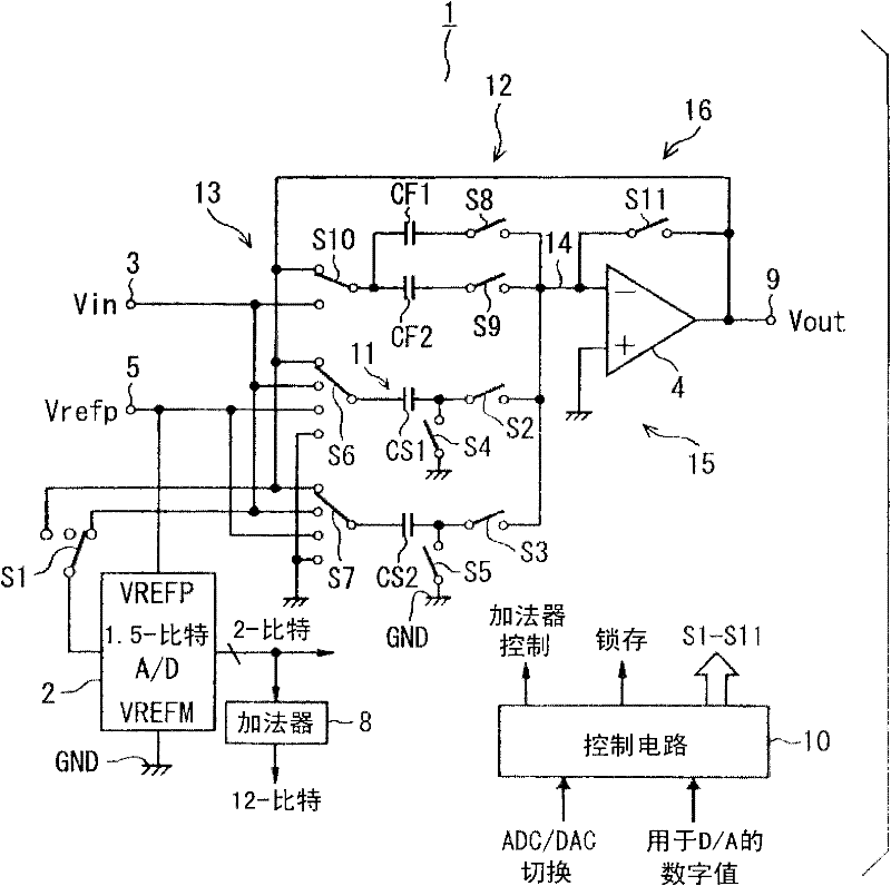
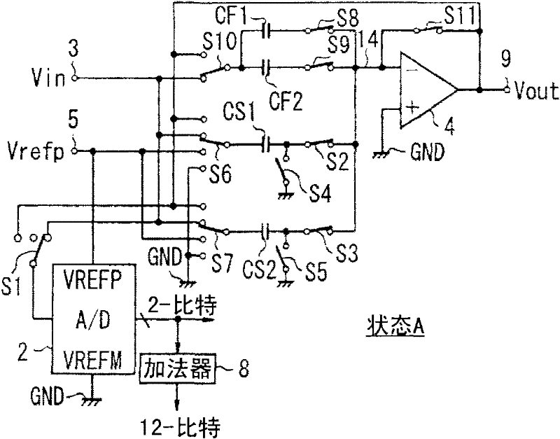
[0030] see figure 1 The cyclic A / D conversion device 1 is provided in, for example, a semiconductor integrated circuit device (IC) mounted in an electronic control unit (ECU) for a vehicle. The cyclic A / D conversion device 1 is configured to perform an A / D conversion operation and a D / A conversion operation. The cyclic A / D conversion device 1 is manufactured using a CMOS process.
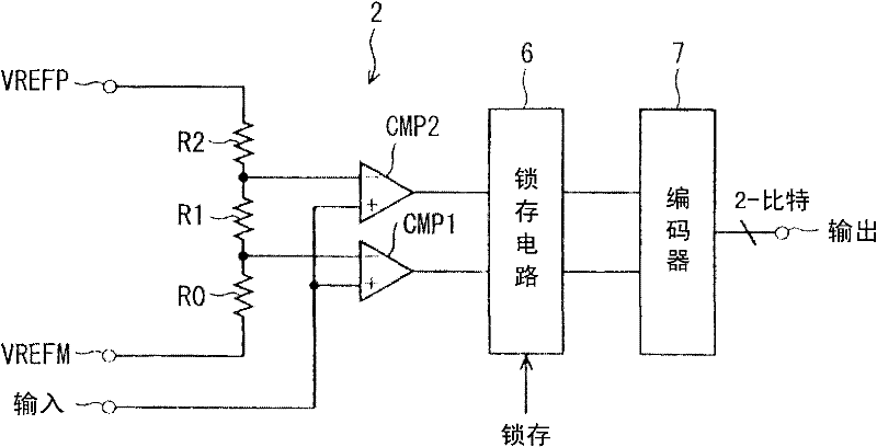
[0031] The input terminal of the parallel A / D conversion circuit 2 with a resolution of 1.5 bits (m=1.5) is selectively connected to one of the signal input terminal 3 and the output terminal of the operational amplifier 4 via the switch S1, or is connected to an unconnected Location. The signal input terminal 3 is supplied with an input signal voltage (external signal voltage) Vin as a target of A / D conversion. When performing an A / D conversion operation, the input terminal of the A / D conversion circuit 2 is selectively connected to one of the signal input terminal 3 and the output terminal of t...
no. 2 example
[0100] Next, refer to Figure 11 to Figure 15 A second embodiment of the present invention is described, wherein the same elements as in the first embodiment are given the same reference numerals.
[0101] see Figure 11 , a cyclic A / D conversion means 31 is provided to perform an A / D conversion operation and a D / A conversion operation, as figure 1 The case of the cyclic A / D conversion device 1 exemplified in . The input terminal of the A / D conversion circuit 2 is selectively connected to one of the signal input terminal 3 and the output terminal of the operational amplifier 4 via a switch S31. Each of the lower electrodes (common-side electrodes) of the capacitors CS1 and CS2 is connected to the common line 32 . The common line 32 is connected to the inverting input terminal of the operational amplifier 4 via the switch S32, and is connected to the ground terminal GND via the switch S33. Upper electrodes (non-common side electrodes) of capacitors CS1 and CS2 are selective...
no. 3 example
[0138] Next, refer to Figure 16 A third embodiment of the present invention is described, wherein the same elements as in the previous embodiments are given the same reference numerals.
[0139] see Figure 16 , cyclic A / D conversion means 41 are provided to perform differential operations. The cyclic A / D conversion device 41 is Figure 11 The differential configuration of the cyclic A / D conversion device 31 exemplified in . A parallel A / D conversion circuit 42 having a resolution of 1.5 bits is configured to perform a differential operation, and an operational amplifier 43 is configured to supply a differential output. The non-inverting input terminal of the A / D conversion circuit 42 is selectively connected to one of the non-inverting signal input terminal 3p and the non-inverting output terminal of the operational amplifier 43 via the switch S31p. Similarly, the inversion input terminal of the A / D conversion circuit 42 is selectively connected to one of the inversion s...
PUM
 Abstract
Description
Claims
Application Information


