Methods of Manufacturing Standard Wafers

A technology for manufacturing standards and wafers, which is applied in the photoengraving process of the pattern surface, the exposure device of the photoengraving process, optics, etc., which can solve the problem of low calibration accuracy of standard wafers, and achieve the effect of small distortion and high calibration accuracy.

Active Publication Date: 2011-12-28
CSMC TECH FAB2 CO LTD
View PDF5 Cites 12 Cited by
  • Summary
  • Abstract
  • Description
  • Claims
  • Application Information

AI Technical Summary

Problems solved by technology

[0007] The problem solved by the present invention is that the calibration accuracy of the standard wafer produced by the prior art is not high

Method used


Image

  • Methods of Manufacturing Standard Wafers
  • Methods of Manufacturing Standard Wafers
  • Methods of Manufacturing Standard Wafers

Examples


Embodiment Construction

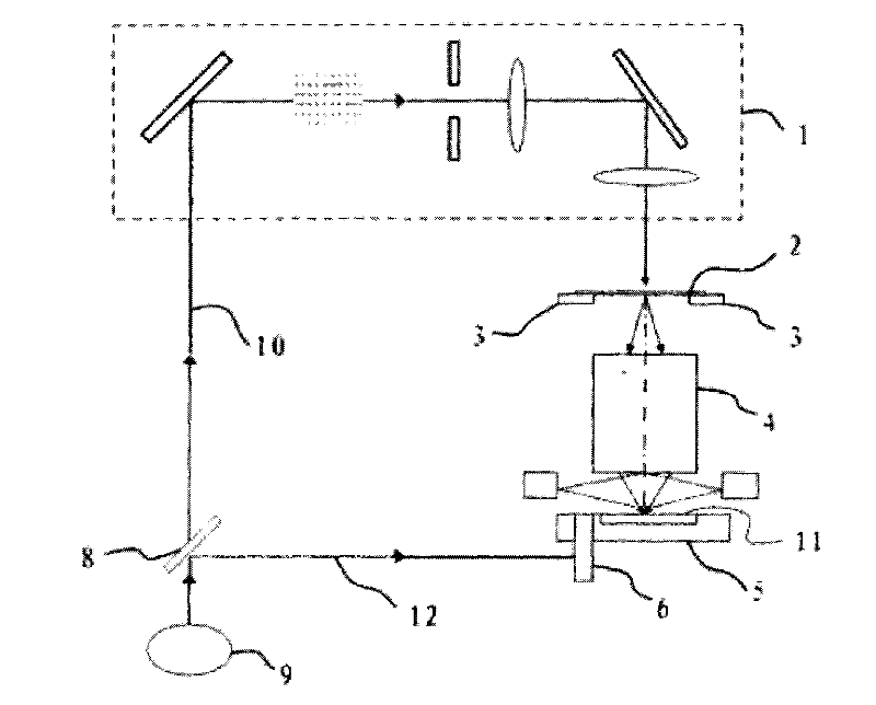
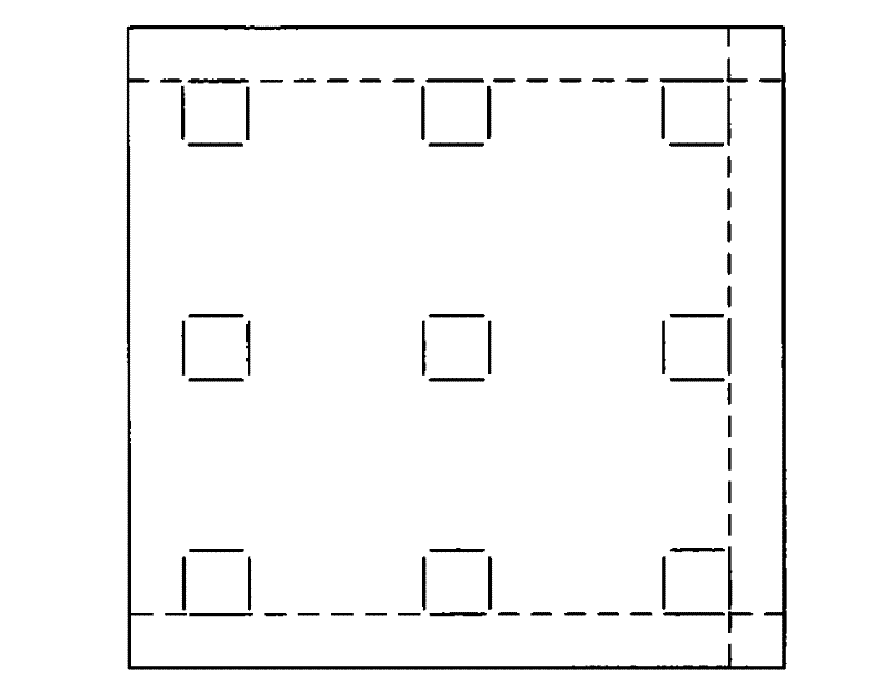
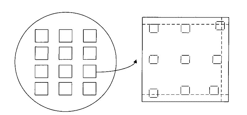
[0027] refer to Figure 4 In the prior art, when performing photolithography, the baffle plate 102 (shown in dotted line) in the photolithography machine exposes all the reference patterns 103 on the photoresist plate 101, and all the reference patterns 103 on the photoresist plate 101 are exposed during photolithography. One exposure. After the first exposure area of ​​the wafer 104 exposes all the patterns 103 on the photoresist plate at one time, the wafer stage of the lithography machine drives the wafer 104 to move to the second exposure area, where the light All the reference patterns 103 on the engraving plate 101 are exposed at one time. In this way, as the wafer stage drives the wafer 104 to move, the exposure of all exposure areas on the entire wafer 104 is completed, and a calibration pattern 105 is formed on the wafer 104, and the wafer 104 with the calibration pattern 105 is used as a standard wafer.

[0028] But when all the reference patterns 103 on the photo...


PUM


Abstract

The invention provides a method for manufacturing a standard wafer. The method comprises the following steps: photoetching a wafer by reference photoetching equipment and exposing a reference pattern on a photomask on the wafer during photoetching to form an alignment pattern on the wafer. The method is characterized in that the reference pattern in the central area of the photomask is only exposed. The method has the following advantages that the standard wafer manufactured by the method is slightly affected by distortion of a projection objective, has high calibration accuracy and can be suitable for all types of photoetching machines; the method has higher flexibility; and the standard wafer manufactured by the method has longer service time.

Description

technical field [0001] The invention relates to the field of semiconductor manufacturing, in particular to a method for manufacturing standard wafers. Background technique [0002] With the development of semiconductor technology, integrated circuits are developing in the direction of high integration. In the chip manufacturing process, multiple photolithography processes are usually required to complete the entire manufacturing process. This requires higher and higher overlay accuracy, which directly affects the yield of integrated circuit products. There are many factors that affect the overlay accuracy, including the shape of the alignment mark on the wafer, the alignment system of the lithography machine, the overlay test equipment, and the distortion of the projection objective lens of the lithography machine. Among them, the distortion of the projection objective lens of the lithography machine is one of the main factors affecting overlay. [0003] In the Chinese pa...

Claims


Application Information

Patent Timeline
Patent Type & Authority Applications(China)
IPC IPC(8): G03F7/20G03F9/00
Inventor 黄玮
Owner CSMC TECH FAB2 CO LTD
Why Eureka
Try Eureka