A metal wiring etching method

A technology of photoresist and photolithographic patterns, which is applied in the direction of electrical components, semiconductor/solid-state device manufacturing, circuits, etc., can solve the problems of the increase of the value of the dielectric coefficient k, dielectric damage, etc., and achieve the reduction of the dielectric coefficient k increase, avoiding the effect of signal transmission speed and

Active Publication Date: 2011-12-28
SEMICON MFG INT (SHANGHAI) CORP +1
View PDF5 Cites 4 Cited by
  • Summary
  • Abstract
  • Description
  • Claims
  • Application Information

AI Technical Summary

Problems solved by technology

Both of the above aspects will cause damage to the low-k interlayer dielectric and increase the value of the dielectric coefficient k

Method used


Image

  • A metal wiring etching method
  • A metal wiring etching method
  • A metal wiring etching method

Examples


specific Embodiment 1

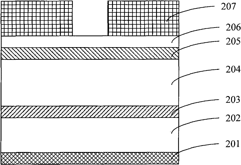
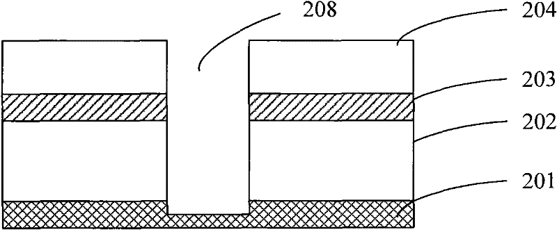
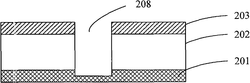
[0037] combined with Figure 3a-3e Details as figure 2 The metal wiring etching method of the present invention shown, its steps are as follows:

[0038] Step 301, Figure 3a It is a schematic cross-sectional structure diagram of step 301 of the metal wiring etching method in the present invention, as Figure 3a As shown, after coating the first photoresist (PR) 407 on the bottom anti-reflective coating (BARC) 406, the first photolithography is used to define the first photolithography pattern for defining the via hole (via);

[0039] In this step, the first photolithography specifically refers to exposing and developing the first PR407 coated on the BARC406 to form a first photolithography pattern. Wherein, the thickness range of coating the first PR407 is 1000 to 3000 angstroms, such as 1000 angstroms, 1500 angstroms and 3000 angstroms; the first photolithography pattern is used to define the opening width of the via holes in the subsequent steps. Figure 3a In the lowe...


PUM

PropertyMeasurementUnit
thicknessaaaaaaaaaa
thicknessaaaaaaaaaa

Abstract

The invention provides a method for etching a metal connecting line. After depositing a first silicon oxide layer and a mask layer on a low dielectric coefficient interlayer dielectric in sequence, the method comprises the following steps: coating a first photoresist to form a first photoetching pattern for defining a through hole; forming a protective layer on the surface of the first photoetching pattern; coating a second photoresist on the protective layer to form a second photoetching pattern for defining a groove; etching to form the through hole and the groove by taking the first photoetching pattern and the second photoetching pattern as masks; ashing and removing mask layer residue after etching, and exposing the first silicon oxide layer. In the method for etching the metal connecting line provided by the invention, once etching is adopted to form the through hole and the groove in the low dielectric coefficient interlayer dielectric, thus reducing the rise of the dielectric coefficient k of the low dielectric coefficient interlayer dielectric caused by the attack of plasma on the low dielectric coefficient interlayer dielectric during the ashing process, and avoiding reducing the signal transmission speed of the semiconductor circuit and the working speed of the semiconductor device.

Description

technical field [0001] The invention relates to a semiconductor manufacturing method, in particular to a metal wiring etching method. Background technique [0002] With the progress of the semiconductor manufacturing process, the area of ​​the semiconductor chip is getting smaller and smaller, and at the same time, the size and the number of semiconductor devices integrated on the same semiconductor chip are getting smaller and smaller. The semiconductor devices are connected by metal wires to form a semiconductor circuit to realize signal transmission between the semiconductor devices. The metal wiring is composed of high-density metal lines and an interlayer dielectric between the metal lines. The resistance capacitance delay phenomenon (Resistance Capacitance Delay, RC Delay) of the metal wiring reduces the signal transmission rate of the semiconductor circuit, thereby reducing the working speed of the semiconductor device. [0003] The signal transmission rate of the s...

Claims


Application Information

Patent Timeline
Patent Type & Authority Applications(China)
IPC IPC(8): H01L21/768
Inventor 张海洋周俊卿
Owner SEMICON MFG INT (SHANGHAI) CORP
Why Eureka
Try Eureka