Micro-optical element for realizing semiconductor laser beam homogenization

A laser beam and micro-optical technology, applied in the field of micro-optical components, can solve the problems of high cost, energy loss, complex installation and adjustment, etc., and achieve the effects of small light energy loss, fewer reflections, and efficient utilization

Inactive Publication Date: 2012-01-04
CHANGCHUN INST OF OPTICS FINE MECHANICS & PHYSICS CHINESE ACAD OF SCI
View PDF4 Cites 7 Cited by
  • Summary
  • Abstract
  • Description
  • Claims
  • Application Information

AI Technical Summary

Problems solved by technology

However, the energy distribution of the beam shaped by this method is very uneven, and there are obvious bright and dark stripes, which need to be homogenized
In terms of homogenization technology, frosted glass is mostly used, but the homogenization effect is not very good, and the energy loss is serious, about 40% to 50%.
There is also a homogenization method using optical fiber, but light homogenization requires an optical coupling device to couple the light from the laser into the optical fiber, which is costly and complicated to install and adjust

Method used


Image

  • Micro-optical element for realizing semiconductor laser beam homogenization
  • Micro-optical element for realizing semiconductor laser beam homogenization
  • Micro-optical element for realizing semiconductor laser beam homogenization

Examples


Embodiment 1

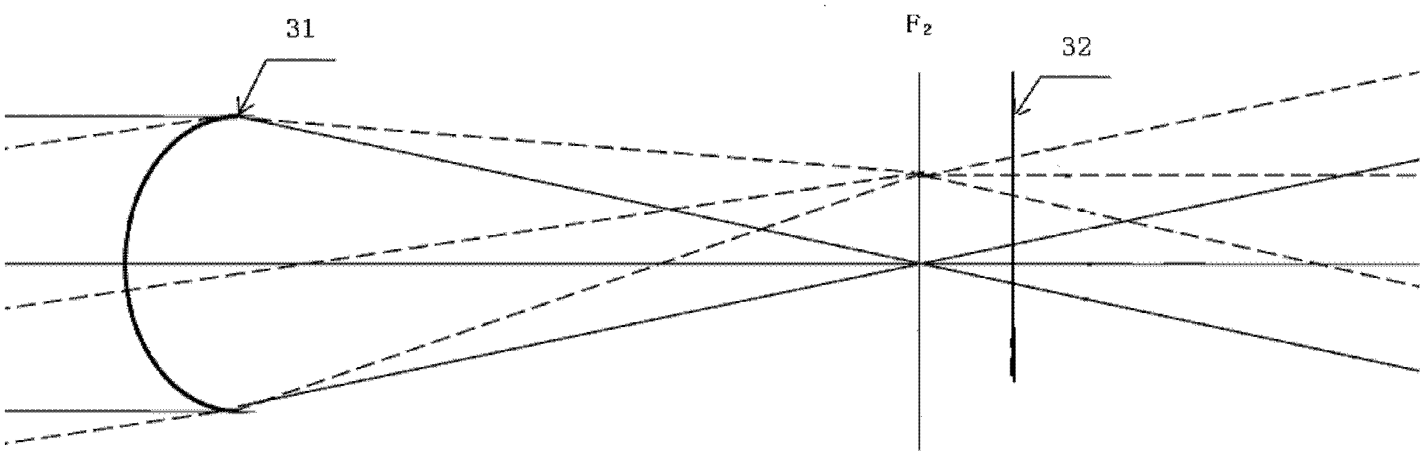
[0031] Such as image 3 As shown, the front surface 31 of the microstructure unit is a spherical surface, and the rear surface 32 is a plane; the semiconductor laser beam after shaping is incident on the front surface 31 of the microstructure unit, and converges into a point light source image in the microstructure unit; the point light source image The emitted light beam is emitted through the rear surface 32 of the microstructure monomer to become divergent light. The divergent light emitted by a series of point light source images in the micro-optical element 3 is superimposed on the illuminating surface.

Embodiment 2

[0033] Such as Figure 4 As shown, the front surface 31 and the back surface 32 of the microstructure unit are spherical surfaces, and the radius of curvature r of the front surface 31 1 less than the radius of curvature r of the rear surface 32 2 The shaped semiconductor laser beam is incident from the front surface 31 of the microstructure monomer, and converges into a point light source image in the microstructure monomer; the light beam emitted by the point light source image is emitted by the rear surface 32 of the microstructure monomer and becomes divergent light. The divergent light emitted by a series of point light source images in the micro-optical element 3 is superimposed on the illuminating surface.

Embodiment 3

[0035] Such as Figure 5 As shown, the front surface 31 and the back surface 32 of the microstructure unit are spherical surfaces, and the radius of curvature r of the front surface 31 1 equal to the radius of curvature r of the rear surface 32 2 It is equal to r; the shaped semiconductor laser beam is incident on the front surface 31 of the microstructure monomer, and converges into a point light source image in the microstructure monomer; the beam emitted by the point light source image passes through the rear surface 32 of the microstructure monomer and becomes divergent light.

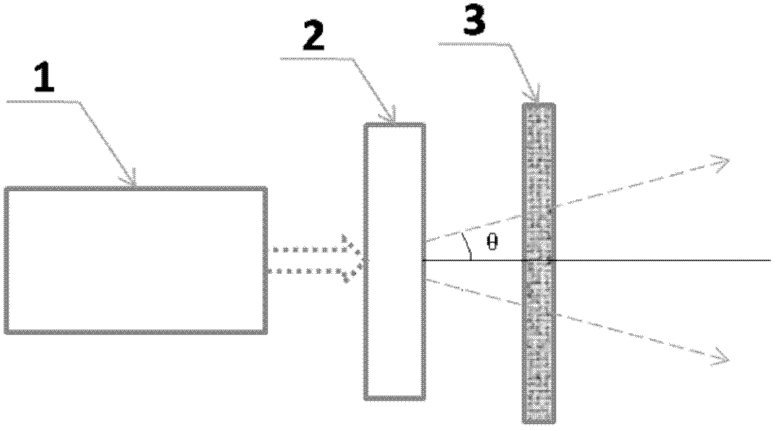
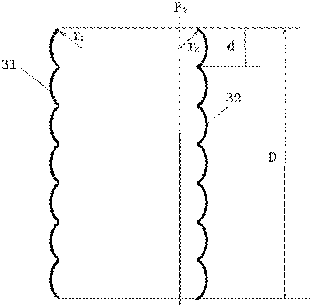
[0036] Before starting the design, we first determine the design parameters: the semi-angle θ of the semiconductor laser beam after passing through the optical shaping element, the aperture D of the laser beam of the micro-optical element, the refractive index n of the material of the micro-optical element, and the arrangement of the micro-structural monomers Way (it can be arranged in a square cl...


PUM


Abstract

The invention relates to a micro-optical element for realizing semiconductor laser beam homogenization, which is composed of a plurality of microstructure monomers arranged in a joint sealing mode, wherein each microstructure monomer comprises a front surface and a back surface, the front surface of each microstructure monomer is a spherical surface; an incident surface of the micro-optical element can be formed by the continuous arrangement of the spherical front surfaces of the plurality of microstructure monomers, and an emergent surface of the micro-optical element can be formed by the continuous arrangement of the back surfaces of the plurality of microstructure monomers; the incident surface of the microstructure element can divide the reshaped semiconductor laser beam into multiplesub-beams, and each sub-beam focuses in the microstructure monomer so as to form a series of point light source images; light beams emitted from the point light source images can leave from the back surfaces of the microstructure monomers; and the divergent light emitted from the back surface of each microstructure monomer can be overlaid on the lighting surface. The micro-optical element provided by the invention has the advantages of high light utilization efficiency, good uniformity effect and low cost and can be widely applied to the field of semiconductor laser lighting, so that the laser illuminators can be better used for night monitoring in the occasions, such as public securities, banks, prisons, forests, etc.

Description

technical field [0001] The invention belongs to the technical field of semiconductor lighting and relates to a micro-optical element for realizing homogenization of semiconductor laser light beams. Background technique [0002] With the improvement of the performance of semiconductor lasers, laser lighting technology based on semiconductor lasers is more and more widely used in the field of safety protection monitoring. Since the beam of the semiconductor laser is an elliptical Gaussian beam, the divergence angles in the horizontal and vertical directions are different, and the spot is uneven. Therefore, semiconductor lasers must be shaped and homogenized before they can be used for night lighting. [0003] At present, the relatively simple shaping technology is to use optical shaping devices such as fiber optic cylindrical mirrors to adjust the horizontal and vertical divergence angles of the laser beam to be basically the same. However, the energy distribution of the bea...

Claims


Application Information

Patent Timeline
IPC IPC(8): G02B27/09
Inventor 刘华卢振武
Owner CHANGCHUN INST OF OPTICS FINE MECHANICS & PHYSICS CHINESE ACAD OF SCI
Why Eureka
Try Eureka