Method for manufacturing electrodes on two surfaces of capacitance touch screen

A production method and capacitive touch technology, applied in the direction of electrical digital data processing, instruments, data processing input/output process, etc., can solve the problems of reduced production costs, high defective products, and easy wear of optical scales, so as to improve production capacity, Simple operation, optimized production flow effect

Inactive Publication Date: 2012-01-18
DONGGUAN RUNHUA OPTOELECTRONICS
View PDF3 Cites 16 Cited by
  • Summary
  • Abstract
  • Description
  • Claims
  • Application Information

AI Technical Summary

Problems solved by technology

[0011] The problem that exists aspect manufacturing technology is: coating photoresist on the front side of substrate, after photoetching, solidification, must coat photoresist protective layer on substrate reverse side, just can carry out positive etching conductive layer; After the photoresist is removed, the photoresist is coated on the reverse side, and after photolithography and curing, it is still necessary to coat the photoresist protective layer on the front side to etch the conductive layer on the back side.
The production cost of this inventive method seems to be reduced, but in actual production, the optical scale is very easy to wear, and the defective products are very high, so the gain outweighs the loss

Method used


Image

  • Method for manufacturing electrodes on two surfaces of capacitance touch screen
  • Method for manufacturing electrodes on two surfaces of capacitance touch screen

Examples


Embodiment Construction

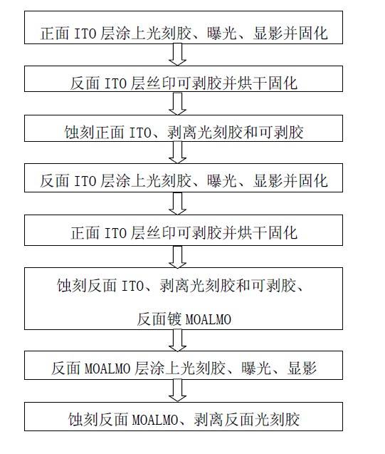
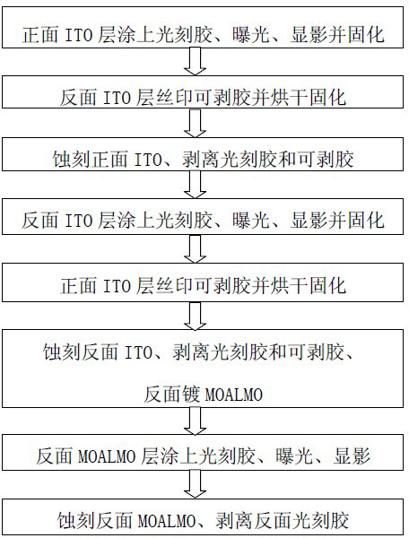
[0028] like figure 1 As shown, a method for manufacturing a capacitive touch screen provided by the present invention is characterized by comprising the following steps:

[0029] The first step: vacuum sputtering the ITO layers 2 and 3 on the substrate, and the thickness of the ITO is 5nm-25nm. The substrate 1 can be made of transparent glass, PET, or organic glass. Apply photoresist on the front ITO layer of the substrate, either by roller coating or by spin coating, so that the thickness of the photoresist can be uniform to about 10%, the thickness is 500-2000nm, and then pre-cured. Pre-curing can be done in a tunnel oven or a hot-air oven. The purpose of pre-curing is to partially cross-link the photoresist, but it must ensure reliable photosensitivity. Temperature condition: 60℃~100℃, time: 120 seconds~3600 seconds, form the resist pattern;

[0030] Step 2: The ITO layer on the reverse side can be screen-printed and peeled off and cured to protect the ITO on the reverse...


PUM


Abstract

The invention discloses a method for manufacturing electrodes on two surfaces of a capacitance touch screen. The method comprises the following steps of: 1, coating a photoresist on a front-surface indium tin oxide (ITO) layer, exposing, developing and curing; 2, silk-screening a peelable adhesive on a back-surface ITO layer, drying, curing, and protecting the back-surface ITO layer; 3, etching the front-surface ITO layer, and peeling the photoresist and the peelable adhesive; 4, coating the photoresist on the back-surface ITO layer, exposing, developing and curing; 5, silk-screening the peelable adhesive on the front-surface ITO layer, drying, curing, and protecting the front-surface ITO layer; 6, etching the back-surface ITO layer to form an ITO pattern or line, peeling the photoresist and the peelable adhesive, and thus obtaining a back-surface molybdenum aluminum molybdenum (MoAlMo) layer by using a film coating line; 7, coating the photoresist on the back-surface MoAlMo layer, exposing and developing to form a pattern; and 8, etching the back-surface MoAlMo layer to form a MoAlMo pattern or line, and peeling the back-surface photoresist. The method has the advantages that: the peelable adhesive replaces the photoresist in the steps 2 and 3, the peelable adhesive is silk-screened by using a silk-screening machine, and a high-cost yellow light line can be used for performing other processes or producing other products; equipment is reasonably utilized; energy production capacity is improved; and cost is reduced.

Description

technical field [0001] The invention relates to a manufacturing method of a touch screen in electronic components, in particular to a manufacturing method of double-sided electrodes of a capacitive touch screen. Background technique [0002] The friendly human-machine interface provided by Apple's iPhone, and the smooth operation performance make the capacitive touch screen sought after by the market, and various capacitive touch screen products have come out one after another. However, with the progress of technology and mass production, its cost continues to drop, and it begins to show a trend of gradually replacing resistive touch screens. Capacitive touch screen can realize multi-point and accurate touch sensing, and has simple structure and high light transmittance, which is the mainstream direction of current display touch technology development. The mainstream direction of touch technology development. The touch sensing component of a capacitive touch screen is gene...

Claims


Application Information

Patent Timeline
Patent Type & Authority Applications(China)
IPC IPC(8): G06F3/044
Inventor 刘明涛
Owner DONGGUAN RUNHUA OPTOELECTRONICS
Why Eureka
Try Eureka