Touch screen with radio built-in antenna, its manufacturing process and electronic device
A technology of built-in antenna and manufacturing process, applied in the direction of antenna support/installation device, electrical digital data processing, input/output process of data processing, etc., can solve problems such as signal interference, achieve low manufacturing cost, reduce thickness, The effect of convenient assembly
- Summary
- Abstract
- Description
- Claims
- Application Information
AI Technical Summary
Problems solved by technology
Method used
Image
Examples
Embodiment 1
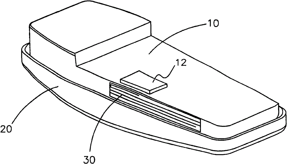
[0047] Such as Figure 4 Shown is a specific embodiment of the touch screen of the present invention, Figure 5for Figure 4 Schematic diagram of the rear view structure, Image 6 for Figure 5 Schematic breakdown of the structure.
[0048] see Figure 4 , Figure 5 and Image 6 , In a specific embodiment of the touch screen of the present invention, it includes a touch layer 10 , a base layer 30 opposite to the touch layer 10 , and a conductive layer 20 between the touch layer 10 and the base layer 30 .
[0049] This embodiment adopts a commonly used resistive touch screen structure (referred to as FG, that is, film-to-glass structure), and its upper layer (ie, the surface facing the user after assembly) is a touch layer 10, and the touch layer 10 is sputtered with ITO (ie, indium Tin oxide) polyester film PET (called ITOFilm in the industry), has certain flexibility and good deformation recovery ability.
[0050] The lower layer of the resistive touch screen structur...
Embodiment 2
[0065] This embodiment is a specific embodiment of the touch screen manufacturing process of the present invention. As mentioned earlier, and referring to Image 6 As shown, the touch screen at least includes a touch layer 10 , a conductive layer 20 and a base layer 30 stacked in sequence.
[0066] In this specific embodiment, firstly, the surface of the base layer 30 facing away from the conductive layer 20 is divided into a first area 33 corresponding to the visible window area 11 of the touch screen, and a second area 34 on the outer surface of the first area 33 .
[0067] Thereafter, an insulating film is printed on the first region 33 by using a process such as screen printing to form an insulating layer. The function of the insulating layer is to provide good working conditions for the subsequent process of processing the conductive path 31 .
[0068] Then, a conductive path 31 is formed in the second region 34 through a magnetron sputtering process, and the conductive...
Embodiment 3
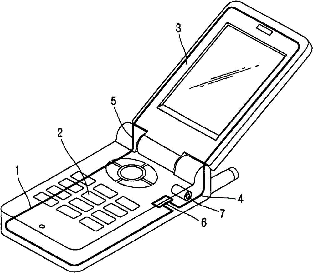
[0073] see Figure 4 and Figure 7 As shown, this embodiment is a specific embodiment of the electronic device of the present invention, and the electronic device described in this embodiment is a mobile phone with a touch screen.
[0074] The touch screen with the built-in radio antenna is installed in the front shell of the mobile phone with the touch layer 10 facing the front shell 1 of the mobile phone.
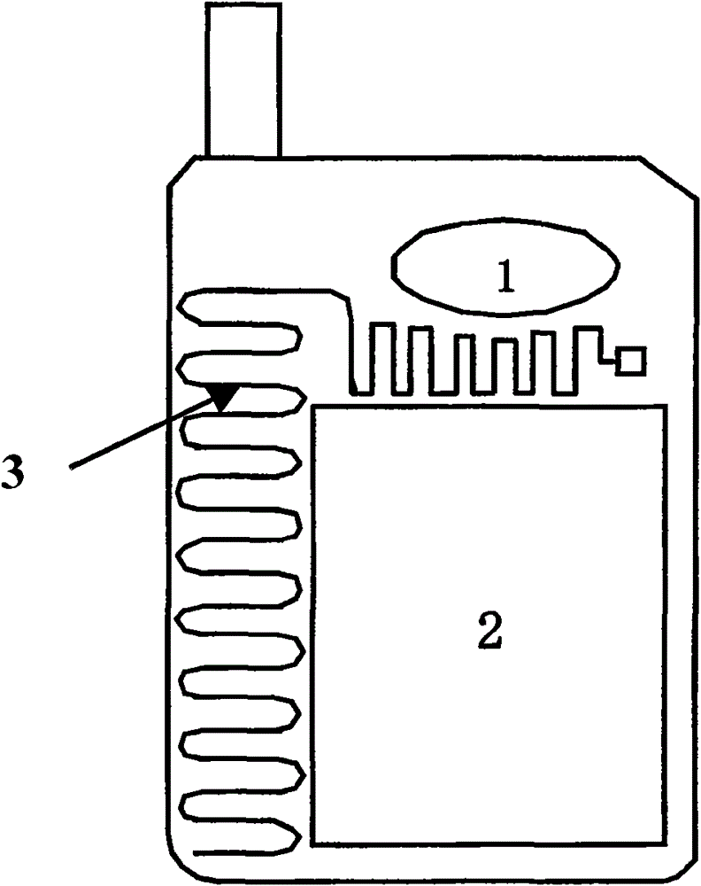
[0075] A mobile phone motherboard is installed on the rear side of the base layer of the touch screen. The radio signal feed point (not shown in the figure) on the main board of the mobile phone connects with the metal shrapnel Figure 5 Connect the radio's antenna feed 32 on the touchscreen as shown in . This completes the connection between the built-in antenna of the radio and the motherboard of the mobile phone.
[0076] Since the mobile phone must also be provided with a mobile phone antenna, in order to overcome the interference of the mobile phone signal and th...
PUM
 Abstract
Description
Claims
Application Information
 - R&D
- Intellectual Property
- Life Sciences
- Materials
- Tech Scout
- Unparalleled Data Quality
- Higher Quality Content
- 60% Fewer Hallucinations
Browse by: Latest US Patents, China's latest patents, Technical Efficacy Thesaurus, Application Domain, Technology Topic, Popular Technical Reports.
© 2025 PatSnap. All rights reserved.Legal|Privacy policy|Modern Slavery Act Transparency Statement|Sitemap|About US| Contact US: help@patsnap.com


