Light emitting semiconductor device with complementary electrode layer and manufacturing method thereof

A technology of light-emitting semiconductor and electrode layer, applied in the direction of semiconductor devices, electrical components, circuits, etc., can solve the problem of easy electrode loss of chips, and achieve the effect of avoiding electrode loss, improving utilization rate and reducing problems.

Active Publication Date: 2017-04-12
LATTICE POWER (JIANGXI) CORP
View PDF7 Cites 0 Cited by
  • Summary
  • Abstract
  • Description
  • Claims
  • Application Information

AI Technical Summary

Problems solved by technology

[0004] The first technical problem to be solved by the present invention is to provide a light-emitting semiconductor device with complementary electrode layers to solve the problem that existing chips are prone to electrode drop
[0005] The second technical problem to be solved by the present invention is to provide a method for manufacturing a light-emitting semiconductor device with complementary electrode layers, which is used to solve the problem that the existing chip is easy to drop electrodes

Method used


Image

  • Light emitting semiconductor device with complementary electrode layer and manufacturing method thereof
  • Light emitting semiconductor device with complementary electrode layer and manufacturing method thereof
  • Light emitting semiconductor device with complementary electrode layer and manufacturing method thereof

Examples


Embodiment Construction

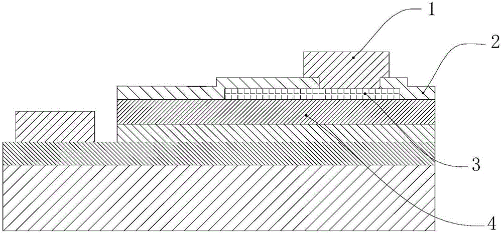
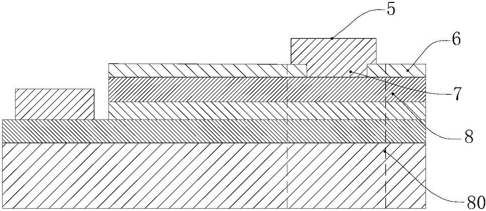
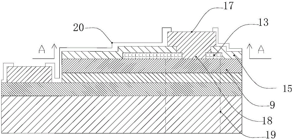
[0032] The present invention proposes a light-emitting semiconductor device with a complementary electrode layer, including a P electrode, a current diffusion layer is formed on the P electrode, a P electrode pad is formed on the current diffusion layer, and an insulating pad is formed under the P electrode pad. layer, the insulating layer is arranged around the electrode pad, and the projection of the P electrode pad is within the projection range of the insulating layer, and is arranged between the current diffusion layer and the P electrode; the P electrode pad is in contact with the P electrode A communication part, which passes through the current diffusion layer and the insulating layer and is in contact with the P electrode.

[0033] The present invention proposes a method for manufacturing a light-emitting semiconductor device with complementary electrode layers, which comprises the following steps: growing a gallium nitride-based semiconductor multilayer structure on a...


PUM


Abstract

The invention discloses a light-emitting semiconductor device with a complementary electrode layer and a manufacturing method thereof, which are used to solve the problem that the existing chips are easy to drop electrodes. The technical solution proposed by the present invention includes a P electrode, a current diffusion layer is formed on the P electrode, a P electrode pad is formed on the current diffusion layer, and an insulating layer is formed under the P electrode pad, and the insulating layer surrounds the The electrode pad is arranged, the projection of the P electrode pad is within the projection range of the insulating layer, and is arranged between the current diffusion layer and the P electrode; the P electrode pad has a communication part in contact with the P electrode, the communication The part is in contact with the P electrode through the current spreading layer and the insulating layer. Under the condition of improving the utilization rate of carriers, the present invention also greatly reduces the problem of falling electrodes, and obviously improves the quality of products.

Description

technical field [0001] The invention relates to an LED semiconductor light emitting device and a manufacturing method thereof. Background technique [0002] The existing sapphire substrate LED structure such as figure 1 As shown, a silicon dioxide insulating layer 3 is made on the P electrode 4, an ITO (indium tin oxide) current spreading layer 2 is made on the silicon dioxide insulating layer 3, and a P electrode pad 1 is made on the current spreading layer 2. , a part of the P electrode pad 1 communicates with the insulating layer 3 . For this sapphire substrate LED device, when the aluminum wire is bonded, the P electrode pad 1 will transmit the external force it receives to the insulating layer 3. Since the insulating layer 3 is made of silicon dioxide, its thickness is very thin, and it is difficult to wire it. The process is easy to break the insulating layer 3, thus causing the problem of electrode drop. [0003] Currently there are also productions such as figur...

Claims


Application Information

Patent Timeline
Patent Type & Authority Patents(China)
IPC IPC(8): H01L33/14H01L33/36H01L33/00
Inventor 管志斌
Owner LATTICE POWER (JIANGXI) CORP
Why Eureka
Try Eureka