Display substrate and method of manufacturing same

一种基底、方向交叉的技术,应用在半导体/固态器件制造、电气元件、电固体器件等方向,能够解决开关元件电气安全性和可靠性降低、电荷迁移率降低、布线电阻率增大等问题,达到改善电学特性的效果

Active Publication Date: 2012-02-08
SAMSUNG DISPLAY CO LTD
View PDF5 Cites 10 Cited by
  • Summary
  • Abstract
  • Description
  • Claims
  • Application Information

AI Technical Summary

Problems solved by technology

Therefore, cations contained in the oxide semiconductor are reduced and extracted, resulting in defect
[0006] When the cations contained in the oxide semiconductor are reduced and extracted, the composition of the channel layer of the TFT is changed so that the charge mobility will decrease
In addition, the resistivity of the wiring will increase due to the metal extracted from the oxide semiconductor
Therefore, the electrical safety and reliability of the switching element will be reduced

Method used


Image

  • Display substrate and method of manufacturing same
  • Display substrate and method of manufacturing same
  • Display substrate and method of manufacturing same

Examples


Embodiment Construction

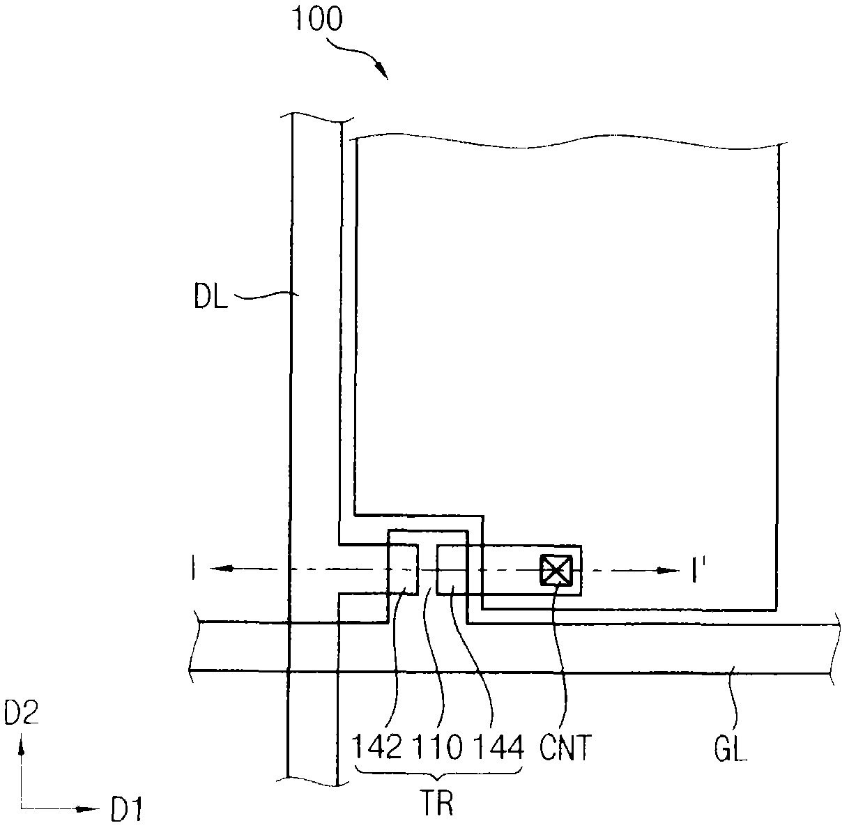
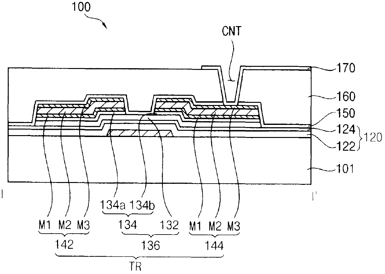
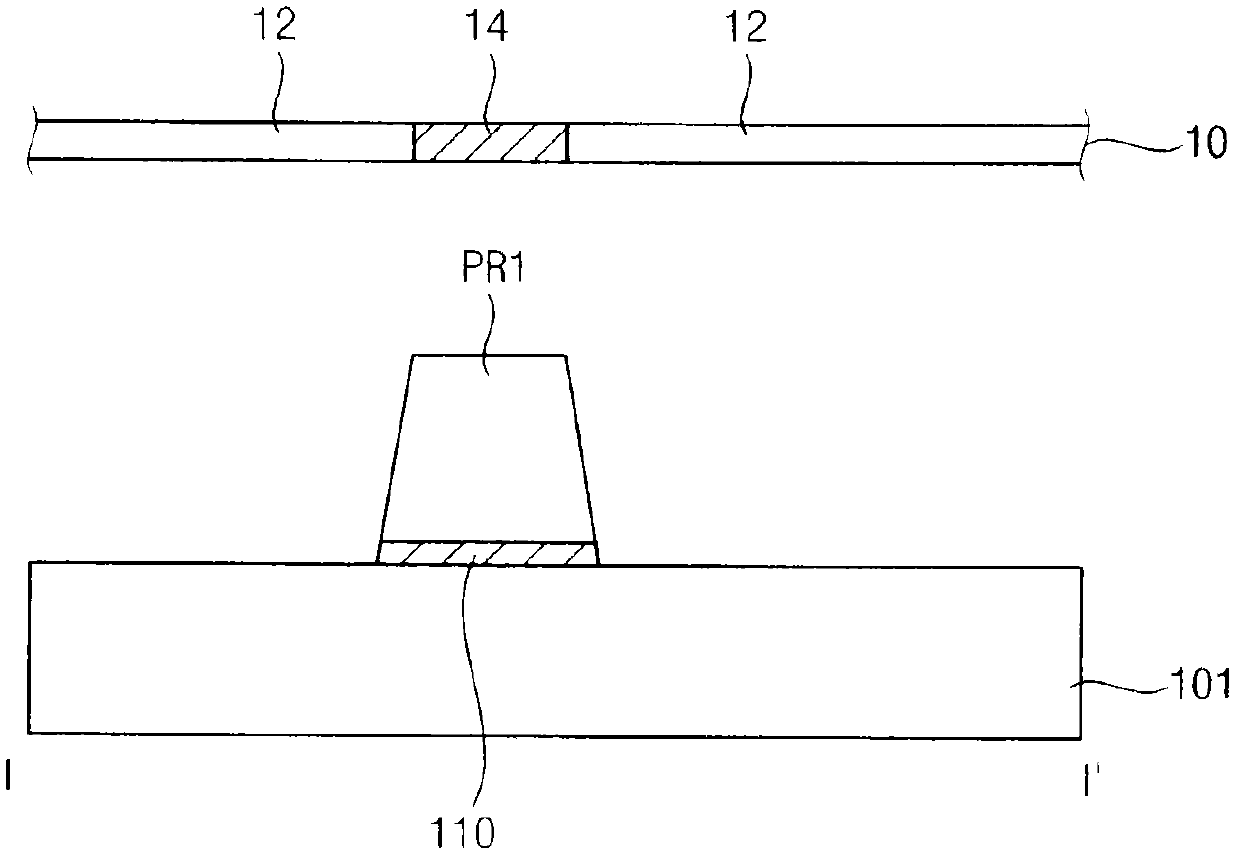
[0034] The present invention is described more fully hereinafter with reference to the accompanying drawings, in which exemplary embodiments of the invention are shown. This invention may, however, be embodied in many different forms and should not be construed as limited to the exemplary embodiments set forth herein. Rather, these embodiments are provided so that this disclosure will be thorough and complete, and will fully convey the scope of the invention to those skilled in the art. In the drawings, the size and relative sizes of layers and regions may be exaggerated for clarity.

[0035] It will be understood that when an element or layer is referred to as being "on" or "connected to" another element or layer, it can be directly on or directly on the other element or layer. is connected to another element or layer, or intervening elements or layers may be present. In contrast, when an element is referred to as being "directly on" or "directly connected to" another eleme...


PUM


Abstract

The invention discloses a display substrate and a method of manufacturing the same. The display substrate includes a gate line extending in a first direction on a base substrate, a data line on the base substrate and extending in a second direction crossing the first direction, a gate insulating layer on the gate line, a thin-film transistor and a pixel electrode. The thin-film transistor includes a gate electrode electrically connected the gate line, an oxide semiconductor pattern, and source and drain electrodes on the oxide semiconductor pattern and spaced apart from each other. The oxide semiconductor pattern includes a first semiconductor pattern including indium oxide and a second semiconductor pattern including indium-free oxide. The pixel electrode is electrically connected the drain electrode.

Description

technical field [0001] The invention relates to a display substrate and a manufacturing method thereof. More particularly, the present invention relates to a display substrate including an oxide semiconductor thin film transistor (TFT) and a method of manufacturing the display substrate. Background technique [0002] Generally, a display device includes an array substrate having switching elements and an opposite substrate opposite to the array substrate. The switching element includes a gate connected to a gate line, a semiconductor pattern insulated from the gate, a source connected to a data line and electrically connected to the semiconductor pattern, and a drain separated from the source. [0003] TFTs used as switching elements of display devices include amorphous silicon TFTs (amorphous Si TFTs), polysilicon TFTs (polycrystalline Si TFTs), oxide semiconductor TFTs, and the like. [0004] Amorphous Si TFTs can be uniformly formed on large substrates at low cost, but ...

Claims


Application Information

Patent Timeline
Patent Type & Authority Applications(China)
IPC IPC(8): H01L27/12H01L21/77
CPCH01L27/1214H01L27/1225H01L29/458H01L27/1288H01L27/124H01L29/45H01L29/7869
Inventor 朴在佑李东勋赵圣行李禹根柳慧英崔永柱
Owner SAMSUNG DISPLAY CO LTD
Why Eureka
Try Eureka