High aspect ratio ultramicro tungsten electrode array and preparation method thereof
A high aspect ratio, tungsten electrode technology, applied in the field of micro-sensing, can solve problems such as difficulty in mass production
- Summary
- Abstract
- Description
- Claims
- Application Information
AI Technical Summary
Problems solved by technology
Method used
Image
Examples
Embodiment Construction
[0029] The present invention will be further described in detail below in conjunction with the accompanying drawings and embodiments.
[0030] 1) Take 5×2 copper splints and tungsten wires with a diameter of 50 μm and clean them with absolute ethanol;
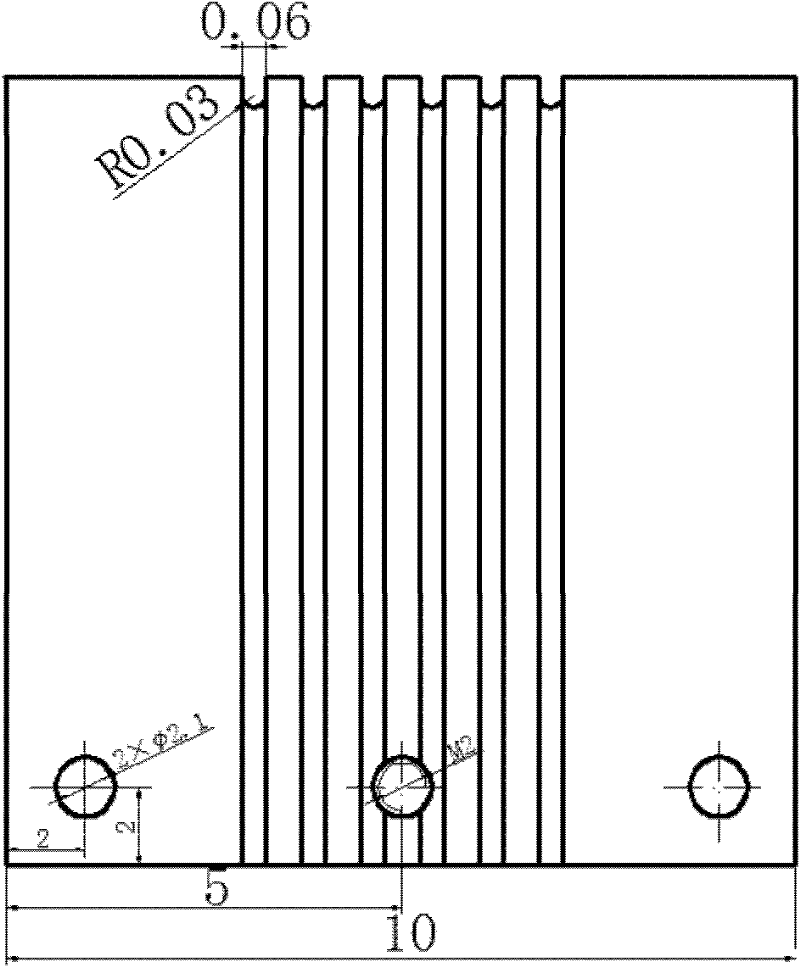
[0031] The size of the copper splint is (10.00, 10.15, 10.30, 10.45, 10.60) mm × 10mm × 2mm;
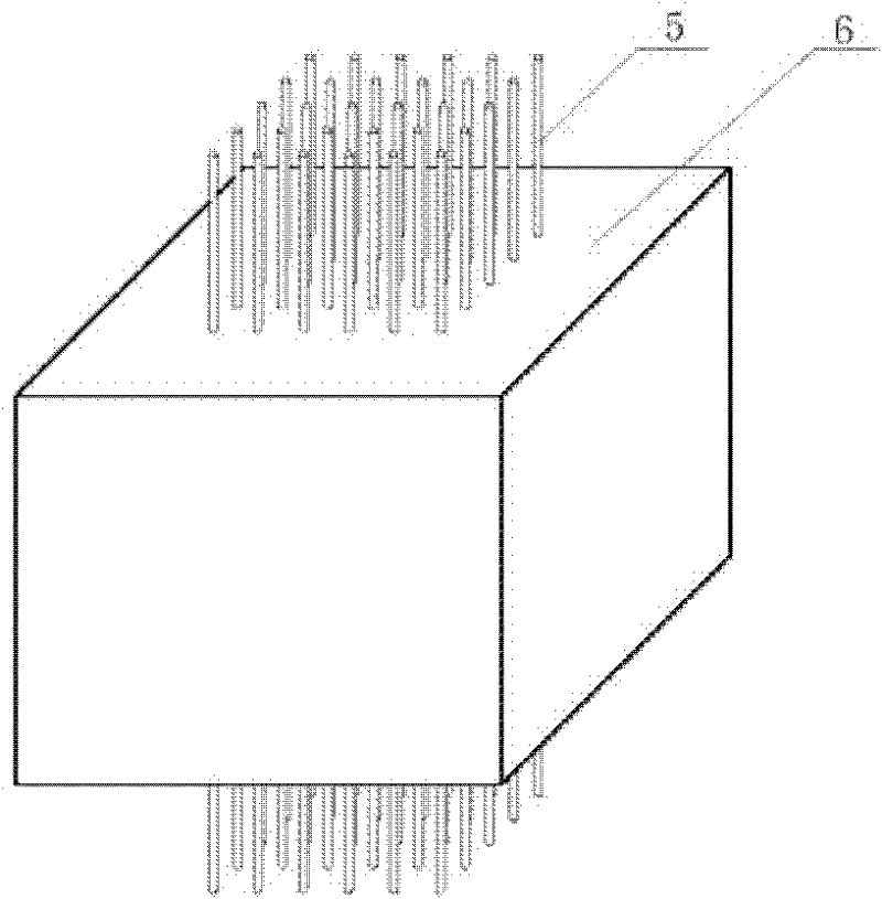
[0032] 2) Referring to Figure 2, use the wire cutting process to symmetrically process 6 copper plates with a width of 60 μm and a depth of The arc groove is 80μm, the distance between adjacent arc grooves is 150μm, the process parameters: no-load voltage 70-90V, peak current <4.8A, pulse width 2-6μs, pulse interval <3μs, wire speed 1m / min, the feed rate is 10mm / min, and the coolant is deionized water;
[0033] 3) Referring to Figure 3, 6 arc grooves with a width of 60 μm and a depth of 6 mm are successively processed from the 15.00 mm sides of two 15mm×10mm×2mm copper plates by wire cutting process, and the distance between adjace...
PUM
| Property | Measurement | Unit |
|---|---|---|
| Diameter | aaaaa | aaaaa |
Abstract
Description
Claims
Application Information


