Semiconductor device and manufacturing method thereof

A manufacturing method and semiconductor technology, applied in the direction of semiconductor/solid-state device manufacturing, semiconductor devices, electrical components, etc., can solve the problems of reduced on-resistance, increased on-resistance, and increased drive current of DEMOS devices, etc., to achieve leakage The source on-resistance value and drive current are kept stable and the effect of improving stability

Active Publication Date: 2012-03-14
SHANGHAI HUAHONG GRACE SEMICON MFG CORP
View PDF7 Cites 2 Cited by
  • Summary
  • Abstract
  • Description
  • Claims
  • Application Information

AI Technical Summary

Problems solved by technology

For example, if the distance S is increased, the on-resistance will increase, thereby reducing the driving current of the DEMOS device; on the contrary, if the distance S is reduced, the on-resistance will be reduced, thereby increasing the driving current of the DEMOS device
[0010] At the same time, in the prior art, after the ion implantation of the lightly doped drain region 11, it is impossible to introduce annealing, such as high-temperature advancement of the furnace tube, so that the implanted ions are redistributed by thermal diffusion.

Method used


Image

  • Semiconductor device and manufacturing method thereof
  • Semiconductor device and manufacturing method thereof
  • Semiconductor device and manufacturing method thereof

Examples


Embodiment Construction

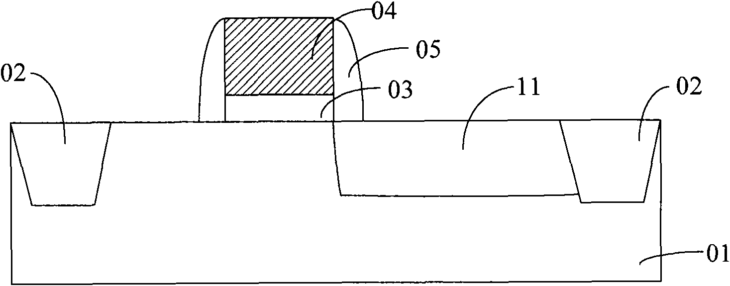
[0044] The present invention covers part of the drain lightly doped region by the gate structure, and uses the gate structure as a mask to perform ion implantation in the drain heavily doped region or the source heavily doped region, so that the drain heavily doped region or the source heavily doped region The distance between the impurity region and the side wall is kept stable, and thus the drain-source on-resistance value and the driving current are kept stable, thereby improving the stability of the manufacturing process of the semiconductor device.

[0045] In order to solve the above problems, the invention provides a method for manufacturing a semiconductor device, such as Image 6 shown, including:

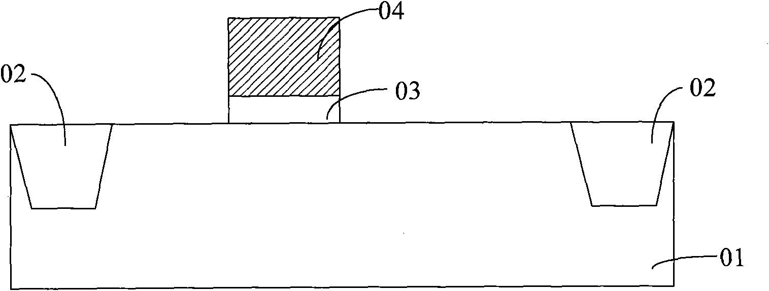
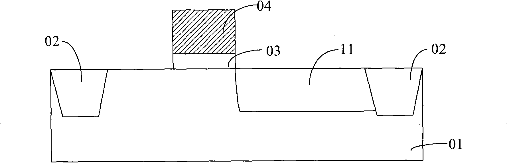
[0046]Step S101, providing a substrate, the substrate includes a vertically extended MOS transistor region, and the substrate has a first conductivity type;

[0047] Step S102, forming a lightly doped drain region in the substrate of the vertically extended MOS transistor...


PUM


Abstract

The invention provides a manufacturing method of a semiconductor device. The method comprises the following steps that: a substrate is provided, wherein the substrate includes a vertical extension MOS transistor region and has a first conductive type; a leak lightly doped region is formed in the substrate of the vertical extension MOS transistor region; a gate structure is formed on the substrate and one side of the gate structure covers a portion of the leak lightly doped region; and a second conductive type ion implantation is carried out on the leak lightly doped region and the substrate by taking the gate structure as a mask layer, so that a leak heavily doped region and a source heavily doped region are formed. According to the invention, a gate structure covers a portion of a leak lightly doped region; and the gate structure is utilized as a mask layer to carry out ion implantation of a leak heavily doped region or a source heavily doped region; therefore, a distance between the leak heavily doped region and a side wall is maintained to be stable; and thus, a leak source conduction resistance value and a drive current are maintained to be stable, so that stability of a manufacturing process of a semiconductor device is improved.

Description

technical field [0001] The invention relates to the field of semiconductor manufacturing, in particular to a semiconductor device and a manufacturing method thereof. Background technique [0002] Extended Drain Metal Oxide Semiconductor (DEMOS) is usually used to make power semiconductor products for high-power switching applications, and has a wide range of applications in liquid crystal panel drive, power management and other fields. [0003] The Chinese patent application with the patent application number 200880008643.3 provides a method for forming the extended drain metal oxide semiconductor (DEMOS), as follows: [0004] Such as figure 1 As shown, a substrate 01 is provided, and the substrate 01 can be single crystal silicon or silicon germanium, or silicon-on-insulator (SOI), or other materials, such as III-V compounds such as gallium arsenide semiconductor. [0005] Wherein, an N-type well and a channel region (not marked) are formed in the substrate 01 . An isol...

Claims


Application Information

Patent Timeline
Patent Type & Authority Applications(China)
IPC IPC(8): H01L21/336H01L21/265H01L29/78H01L29/36
Inventor 邵丽巨晓华
Owner SHANGHAI HUAHONG GRACE SEMICON MFG CORP
Why Eureka
Try Eureka