Silicon through hole technology

A technology of through-silicon vias and processes, which is applied in the fields of electrical components, semiconductor/solid-state device manufacturing, circuits, etc. It can solve problems such as polymer and particle residue, through-hole failure, etc., and achieve the effect of improving reliability and product yield

Inactive Publication Date: 2012-03-14
SHANGHAI HUALI MICROELECTRONICS CORP
View PDF4 Cites 5 Cited by
  • Summary
  • Abstract
  • Description
  • Claims
  • Application Information

AI Technical Summary

Problems solved by technology

[0005] The technical problem to be solved by the present invention is to provide a through-silicon via process to solve the problem that the through-hole fails due to polymer and particles remaining in the through-hole due to high aspect ratio

Method used


Image

  • Silicon through hole technology
  • Silicon through hole technology
  • Silicon through hole technology

Examples


Embodiment Construction

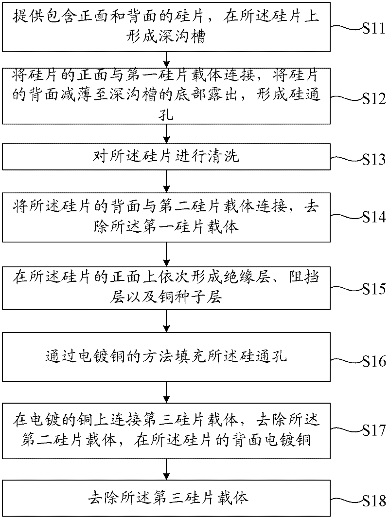
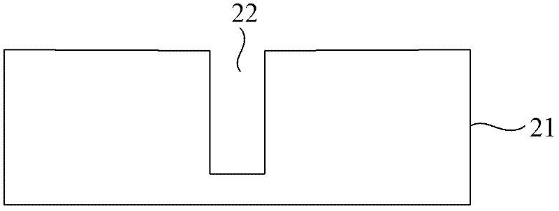
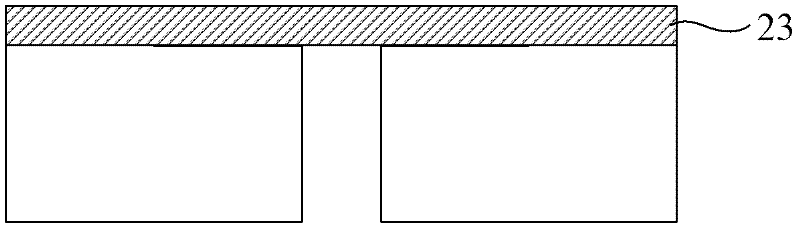
[0015] A TSV process proposed by the present invention will be further described in detail below with reference to the accompanying drawings and specific embodiments. Advantages and features of the present invention will be apparent from the following description and claims. It should be noted that all the drawings are in very simplified form and use imprecise ratios, which are only used for the purpose of conveniently and clearly assisting in describing the embodiments of the present invention.

[0016] The core idea of ​​the present invention is that the provided TSV process thins the backside of the silicon wafer until the bottom of the deep trench is exposed to form a TSV, and cleans the silicon wafer to better remove the TSV. Polymers and particles, thereby improving the reliability of TSVs and ultimately improving product yield.

[0017] figure 1 It is a flow chart of the steps of the TSV process provided by the embodiment of the present invention. refer to figure 1 ...


PUM

PropertyMeasurementUnit
diameteraaaaaaaaaa
depthaaaaaaaaaa

Abstract

The invention provides a silicon through hole technology comprising the steps of: providing a silicon slice with a front surface and a back surface, wherein a deep slot is formed on the silicon slice; connecting the front surface of the silicon slice with a first silicon slice carrier, thinning the back surface of the silicon slice until the bottom of the deep slot is exposed so as to form a silicon through hole; cleaning the silicon slice; connecting the back surface of the silicon slice with a second silicon slice carrier, and removing the first silicon slice carrier; sequentially forming an insulation layer, a barrier layer and a copper seed layer on the front surface of the silicon slice; filling the silicon through hole by electroplating copper; connecting a third silicon carrier on the electroplated copper, removing the second silicon carrier, and electroplating copper on the back surface of the silicon slice; and removing the third silicon slice carrier. According to the silicon through hole technology provided by the invention, the back surface of the silicon slice is thinned until the bottom of the deep slot is exposed so as to form the silicon through hole, and the silicon slice is cleaned so as to remove polymer and particles in the through hole much better, therefore, the reliability of the silicon through hole is enhanced, and finally the product yield is increased.

Description

technical field [0001] The invention relates to the technical field of manufacturing semiconductor integrated circuits, in particular to a through-silicon via process. Background technique [0002] As the integration level of integrated circuits continues to increase, semiconductor technology continues to develop rapidly. The existing integration improvement is mainly to reduce the minimum feature size, so that more components can be integrated in a given area. However, the above-mentioned reduced minimum feature sizes are basically 2D (two-dimensional) integration in essence. Specifically, the integrated components are all located on the surface of the semiconductor wafer (wafer). Even after the 22nm technology platform, system complexity and equipment investment costs have risen sharply, making the use of modern electronic packaging technology to achieve high-density 3D (three-dimensional) integration, becoming an important technical approach for system-level integration ...

Claims


Application Information

Patent Timeline
Patent Type & Authority Applications(China)
IPC IPC(8): H01L21/768
Inventor 周军傅昶
Owner SHANGHAI HUALI MICROELECTRONICS CORP
Why Eureka
Try Eureka