Unit structure of MTP (Multi-Time Programmable) device

A cell structure and device technology, applied in the NVM field, can solve the problems of increasing the erasing voltage, increasing the memory cell area of ​​MTP devices, and punching through.

Active Publication Date: 2012-03-14
SHANGHAI HUAHONG GRACE SEMICON MFG CORP
View PDF4 Cites 13 Cited by
  • Summary
  • Abstract
  • Description
  • Claims
  • Application Information

AI Technical Summary

Problems solved by technology

But increasing the erase voltage can easily cause punch through
In order to avoid punch-through, it is necessary to increase the spacing between the n-wells (that is, increase the critical dimensions c1 and c2), which in turn increases the area of ​​the memory cell of the MTP device

Method used


Image

  • Unit structure of MTP (Multi-Time Programmable) device
  • Unit structure of MTP (Multi-Time Programmable) device
  • Unit structure of MTP (Multi-Time Programmable) device

Examples


Embodiment Construction

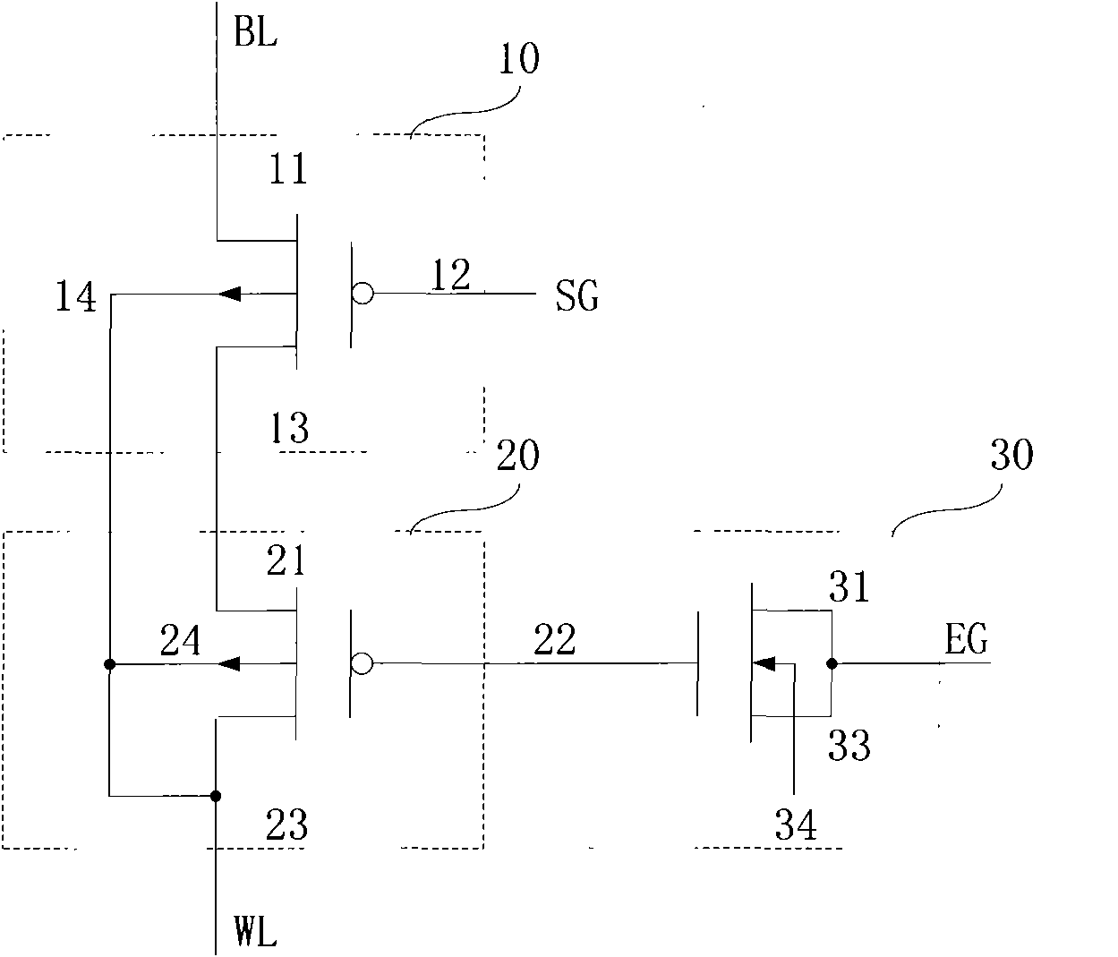
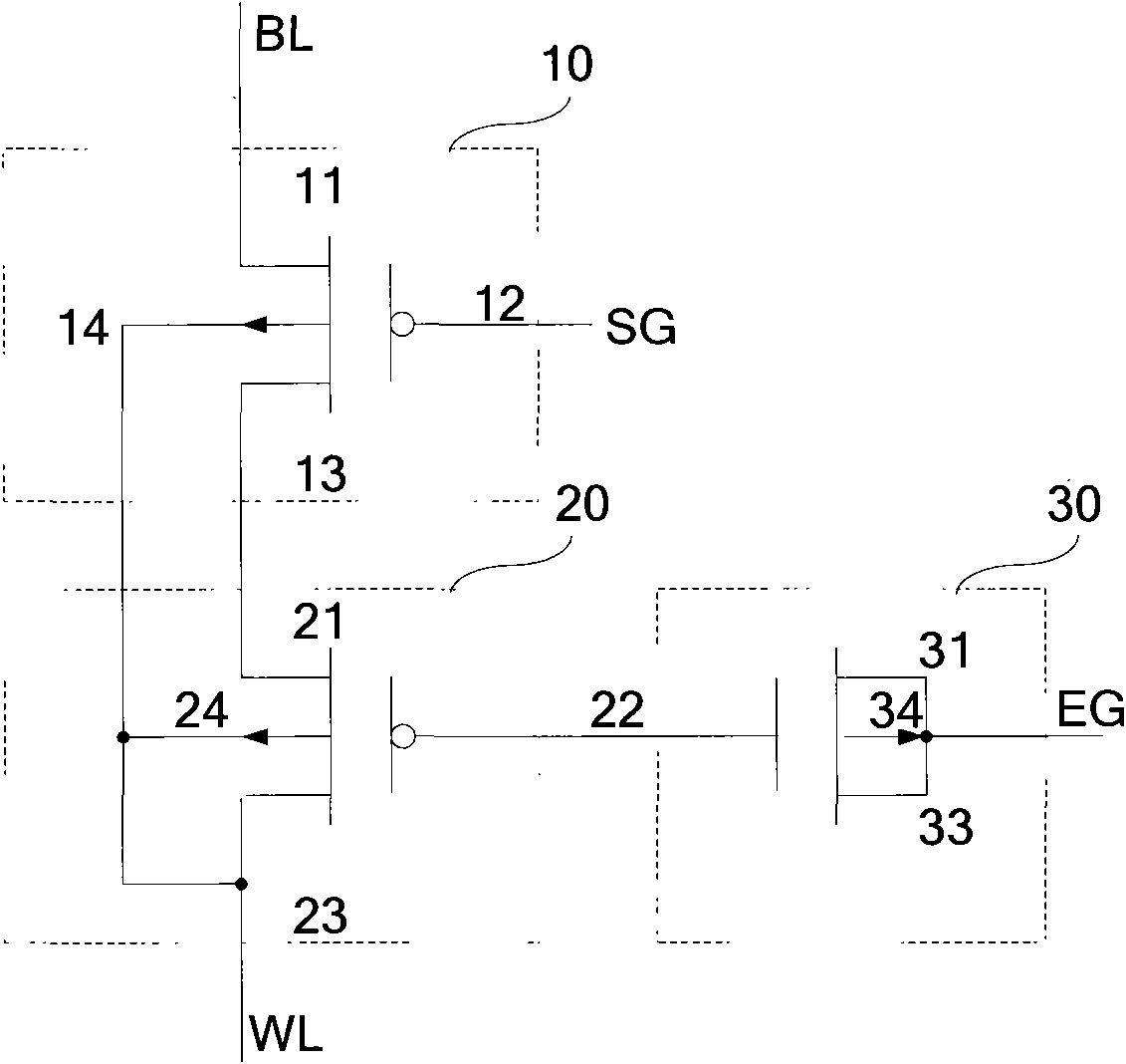
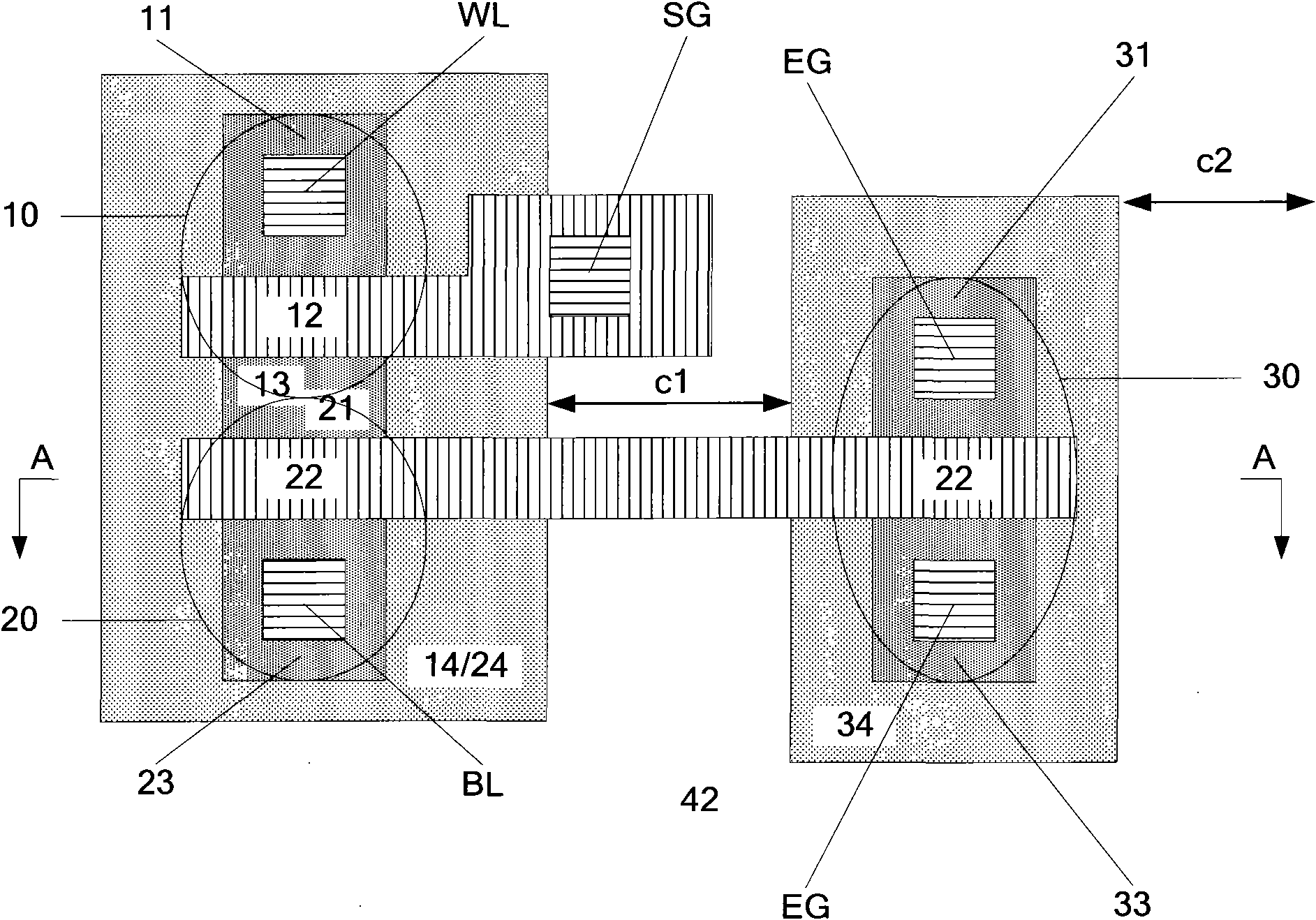
[0025] see Figure 5 , the unit structure of the MTP device of the present invention includes a selection transistor 10 , a programming transistor 20 and an erasing capacitor 50 . The selection transistor 10 and the programming transistor 20 are located in the same n-well 24 . The source 11 of the selection transistor 10 is used as the drain BL, the gate 12 of the selection transistor 10 is used as the selection terminal SG, and the drain 13 of the selection transistor 10 is connected to the source 21 of the programming transistor 20 . The gate 22 of the programming transistor 20 extends outward to form a floating gate, and the floating gate 22 serves as the lower plate of the erasing capacitor 50 . The drain 23 of the programming transistor 20 is connected to the n-well 24 as the programming terminal WL. The upper plate 51 of the erasing capacitor 50 is made of metal, and the metal upper plate 51 of the erasing capacitor 50 serves as the erasing terminal EG.

[0026] The m...


PUM


Abstract

The invention discloses a unit structure of an MTP (Multi-Time Programmable) device. The unit structure comprises a selection transistor, a programming transistor and an erasure capacitor, wherein the selection transistor and the programming transistor are located in the same n well; a source electrode of the selection transistor is used as a drain end, and a gate electrode of the selection transistor is used as a selection end; a drain electrode of the selection transistor is connected with the source electrode of the programming transistor; the gate electrode of the programming transistor extends out to form a floating gate; the floating gate is used as a lower polar plate of the erasure capacitor; the drain electrode of the programming transistor is connected with the n well to be used as a programming end; and an upper polar plate of the erasure capacitor is made of metal and used as an erasure end. The unit structure of the MTP device can be used for obviously reducing a layout area of the unit structure of the MTP device and obviously increasing the erasure voltage, therefore, the erasure speed is improved and the error programming is reduced.

Description

technical field [0001] The present invention relates to an NVM (Non Volatile Memory, non-volatile memory), in particular to an MTP (Multi-Time Programmable, multi-programmable) NVM device. Background technique [0002] see figure 1 , which is a cell structure of an existing MTP device. It includes a selection transistor 10 , a programming transistor 20 and an erasing transistor 30 , which are respectively located in the n well 14 , n well 24 and n well 34 . The source 11 of the selection transistor 10 is used as the drain BL, the gate 12 of the selection transistor 10 is used as the selection terminal SG, and the drain 13 of the selection transistor 10 is connected to the source 21 of the programming transistor 20 . The gate of the program transistor 20 and the gate of the erase transistor 30 are the same floating poly (floating poly) 22 . The drain 23 of the programming transistor 20 , the n-well 14 , and the n-well 24 are connected to each other and serve as the program...

Claims


Application Information

Patent Timeline
IPC IPC(8): H01L27/115H01L29/06H01L29/41
Inventor 胡晓明
Owner SHANGHAI HUAHONG GRACE SEMICON MFG CORP
Why Eureka
Try Eureka