
Magnetic tunnel junction memory unit and manufacturing method thereof

A storage unit and magnetic channel technology, which is applied in the manufacture/processing of electromagnetic devices, electrical components, and parts of electromagnetic equipment, etc., can solve problems such as the failure of magnetic channel junction storage units, and achieve the effect of preventing pollution and damage.

Active Publication Date: 2013-12-11
SEMICON MFG INT (SHANGHAI) CORP +1
View PDF5 Cites 0 Cited by
  • Summary
  • Abstract
  • Description
  • Claims
  • Application Information

AI Technical Summary

Problems solved by technology

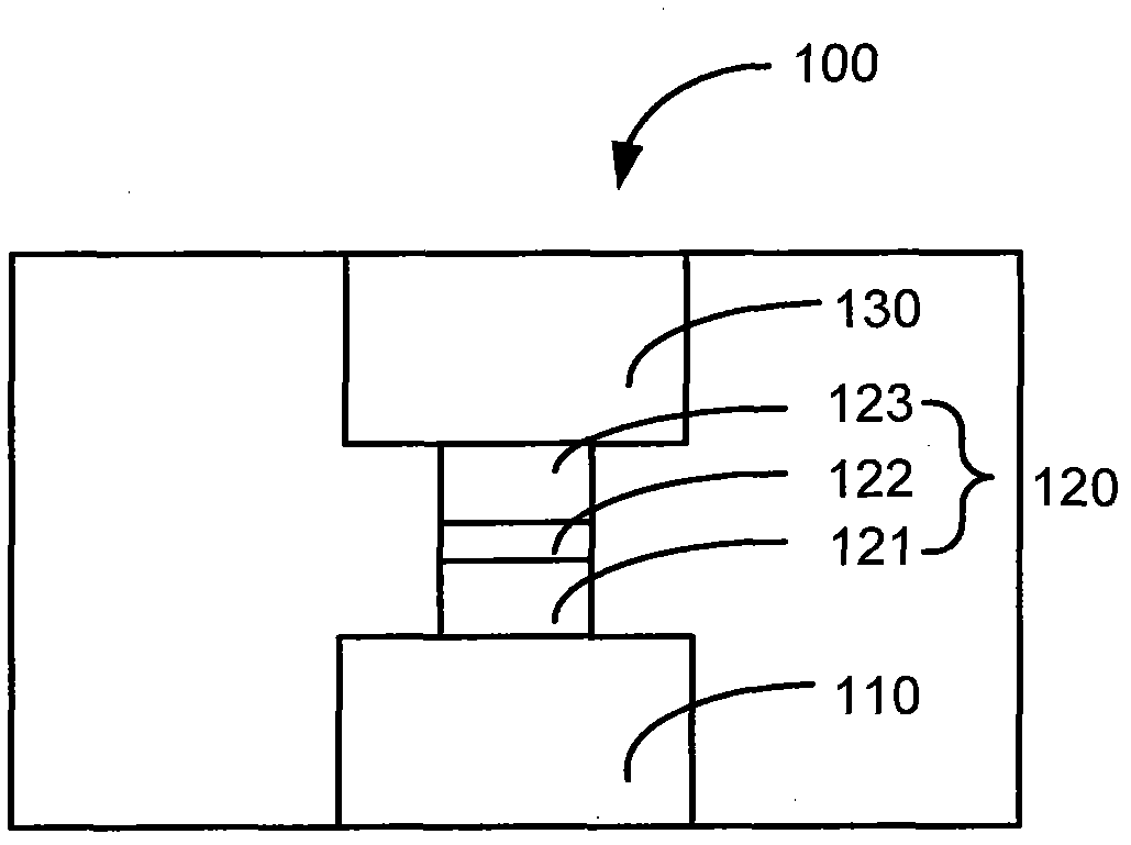
This may cause electrical connection between the lower electrode 110 and the subsequently formed upper electrode due to a defect in the dielectric layer, resulting in failure of the magnetic channel junction memory cell
[0007] Therefore, there is a need for a magnetic channel junction memory cell and its manufacturing method, which can overcome the problem of electrical connection between the upper and lower electrodes due to the defect of the dielectric layer without increasing the line width of the magnetic channel junction, thereby avoiding magnetic channel junction memory cell failure

Method used


Image

  • Magnetic tunnel junction memory unit and manufacturing method thereof
  • Magnetic tunnel junction memory unit and manufacturing method thereof
  • Magnetic tunnel junction memory unit and manufacturing method thereof

Examples


Embodiment Construction

[0031] In the following description, numerous specific details are given in order to provide a more thorough understanding of the present invention. It will be apparent, however, to one skilled in the art that the present invention may be practiced without one or more of these details. In other examples, some technical features known in the art are not described in order to avoid confusion with the present invention.

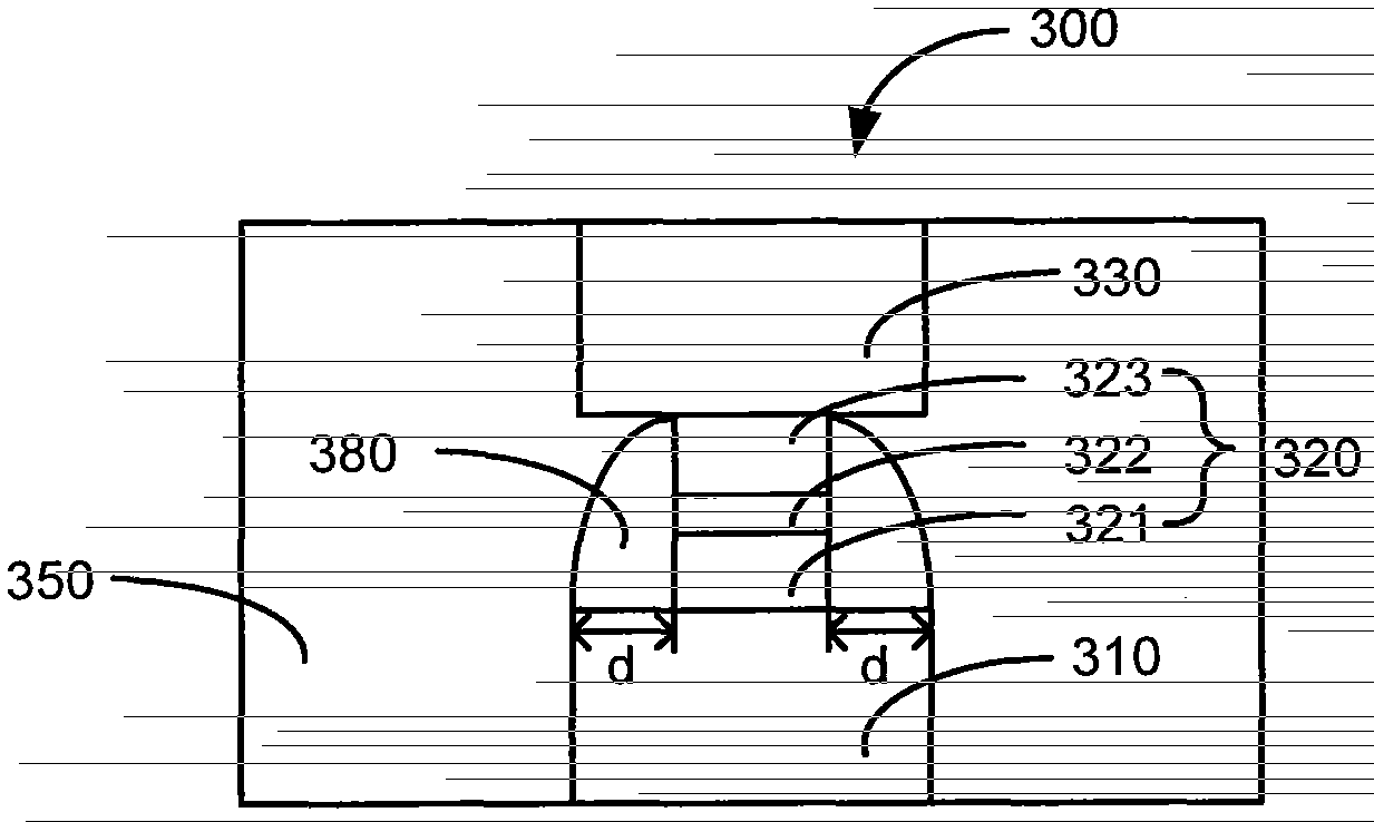
[0032] In order to thoroughly understand the present invention, the detailed structure and steps will be proposed in the following description, so as to illustrate the magnetic channel junction memory cell and its manufacturing method of the present invention, so as to avoid the electrical connection between the upper and lower electrodes due to the defect of the dielectric layer . Obviously, the practice of the invention is not limited to specific details familiar to those skilled in the semiconductor arts. Preferred embodiments of the present invention are d...


PUM


Abstract

The invention relates to a magnetic tunnel junction memory unit and a manufacturing method thereof. The magnetic tunnel junction memory unit comprises a lower electrode, an upper electrode, a magnetic tunnel junction and a side wall structure, wherein the upper electrode is arranged above the lower electrode; the magnetic tunnel junction is sandwiched between the lower electrode and the upper electrode; and the side wall structure is formed on two sides of the magnetic tunnel junction. According to the magnetic tunnel junction memory unit provided by the invention, on the premise that the line width of the magnetic tunnel junction is not increased, the problem of electric connection formed between the upper and lower electrodes caused by defect of a dielectric layer can be overcome, thereby avoiding failure of the magnetic tunnel junction memory unit.

Description

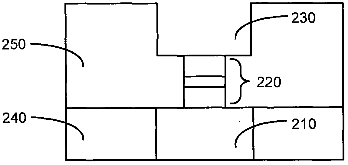
technical field [0001] The invention relates to a semiconductor memory, in particular to a magnetic channel junction (MTJ) storage unit, a magnetic random access memory (MRAM) with the magnetic channel junction storage unit and a manufacturing method of the magnetic channel junction storage unit. Background technique [0002] Magnetic random access memory (Magnetic Random Access Memory, MRAM) is a kind of static random access memory, which has high-speed reading and writing capabilities, and high integration of dynamic random access memory, and can basically be repeatedly written infinitely. The MRAM includes a transistor and a magnetic tunnel junction (Magnetic Tunnel Junction, MTJ) memory cell for storing data. MRAM is a memory device that utilizes the properties of these MTJ cells to write data. [0003] figure 1 A schematic structural diagram of a magnetic channel junction memory cell in the prior art is shown. The magnetic channel junction memory cell 100 includes a ...

Claims


Application Information

Patent Timeline
Patent Type & Authority Patents(China)
IPC IPC(8): H01L43/02H01L43/12H01L27/22H10N50/80H10N50/01
Inventor 韩秋华张海洋胡敏达
Owner SEMICON MFG INT (SHANGHAI) CORP
Learn More