Coaxial probe for wafer probe cards and spider using same

A coaxial probe and probe card technology, applied in the direction of single semiconductor device testing, measuring electricity, measuring devices, etc., can solve the problems of instability and short circuit of capacitive and inductive coupling test, and achieve the stability and avoidance of short circuit. Effect

Inactive Publication Date: 2012-03-21
陈 建宏 +1
View PDF4 Cites 14 Cited by
  • Summary
  • Abstract
  • Description
  • Claims
  • Application Information

AI Technical Summary

Problems solved by technology

However, during the test, the capacitive and inductive coupling between the probes is likely

Method used


Image

  • Coaxial probe for wafer probe cards and spider using same
  • Coaxial probe for wafer probe cards and spider using same
  • Coaxial probe for wafer probe cards and spider using same

Examples


Embodiment Construction

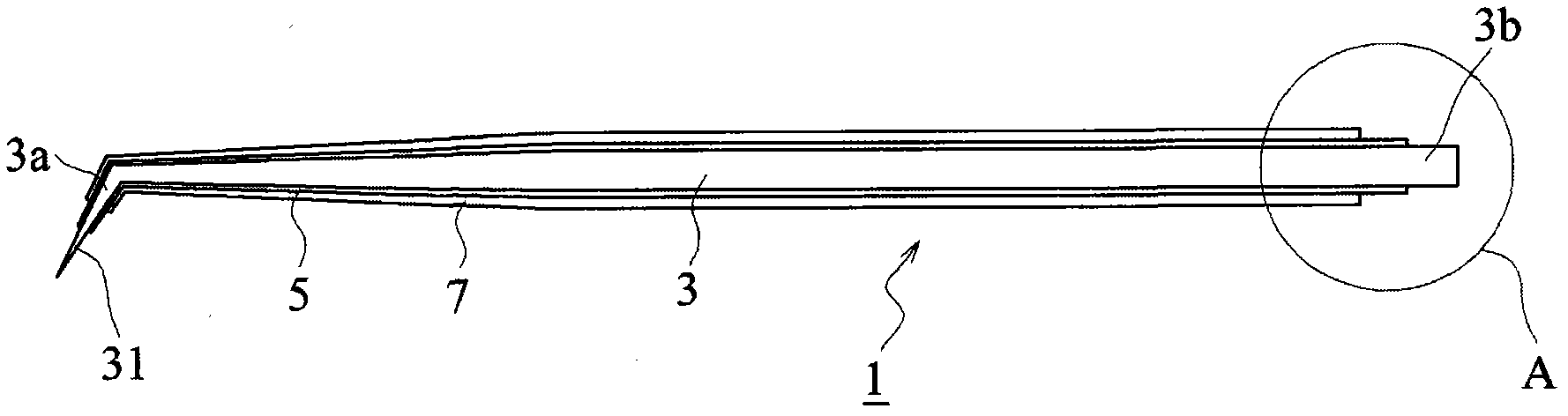
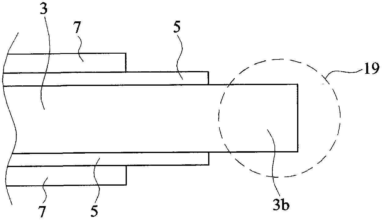
[0051] Figure 1A is a schematic cross-sectional view of a coaxial probe according to an embodiment of the present invention. Such as Figure 1A As shown, the coaxial probe 1 comprises: a tungsten or tungsten alloy probe body 3; one or more layers of insulating layer 5 deposited on a region of the probe body 3; and a metal conductive layer 7 deposited on at least a part of a Or multi-layer insulating layer 5. The probe body 3 has a first end 3 a and a second end 3 b, wherein the first end 3 a is inclined relative to the probe body 3 and has a tip 31 . Such as Figure 1A As shown, the area where one or more insulating layers 5 are deposited does not cover the tip 31 of the first end 3 a and the second end 3 b of the probe body 3 . The conductive metal layer 7 may be deposited to completely or partially cover the insulating layer 5 deposited on this area, ie, the conductive metal layer 7 may be deposited on at least a part of the insulating layer 5 . One or more insulating lay...


PUM


Abstract

The invention provides a coaxial probe for wafer probe cards and a spider using the same, wherein the coaxial probe for wafer probe cards comprises a tungsten or tungsten alloy probe body, one or more insulating layers and a metal conducting layer; the tungsten or tungsten alloy probe body is provided with a first end and a second end, wherein the first end is inclined relative to the probe body and provided with a tip; the insulating layers are deposited on one area of the probe body, wherein the area does not cover the tip of the first end and the second end; and the metal conducting layer is deposited on at least one part of the insulating layers. By means of the invention, the noise produced by the capacitive and inductive coupling between the probes can be shielded, the stability of a test is guaranteed when the test is carried out, and short-circuiting is prevented.

Description

technical field [0001] The present invention relates to a coaxial probe of a wafer probe card and a test head (spider) using the coaxial probe, in particular to a coaxial probe of a wafer probe card that can effectively provide noise shielding and a test head using the coaxial probe. Background technique [0002] Wafer needle testing technology has been evolving along with the semiconductor process technology, and it is also being used continuously, so that the quality of the bare die can be tested after dicing and before packaging, so as to avoid the packaging cost of defective products. In recent years, semiconductor process technology has advanced by leaps and bounds. At this stage, the channel length of transistors has evolved from 0.15 microns to 0.13 microns to the latest 90-nanometer process. ICs are getting smaller and stronger, and the number of pins is getting higher and higher. more. Therefore, the number of probes and the density of probes of the probe card are...

Claims


Application Information

Patent Timeline
IPC IPC(8): G01R1/067G01R31/26
Inventor 陈建宏张智泓
Owner 陈 建宏
Why Eureka
Try Eureka