Solar wafer and preparation method thereof

A technology of solar wafers and wafers, which is applied in the fields of final product manufacturing, sustainable manufacturing/processing, electrical components, etc., and can solve problems such as difficult doping uniformity and dose control, difficulty in achieving solar conversion efficiency, etc.

Active Publication Date: 2013-07-31
KINGSTONE SEMICONDUCTOR LIMITED COMPANY
View PDF6 Cites 0 Cited by
  • Summary
  • Abstract
  • Description
  • Claims
  • Application Information

AI Technical Summary

Problems solved by technology

The solar energy conversion efficiency of this method is improved compared with the doping method of P-type substrate wafer thermal diffusion method, but due to the limitation of the solid solubility of doping by the thermal diffusion method and the difficulty in accurately controlling the doping uniformity and dosage, the actual product It is difficult to achieve the solar energy conversion efficiency of laboratory theory

Method used


Image

  • Solar wafer and preparation method thereof
  • Solar wafer and preparation method thereof
  • Solar wafer and preparation method thereof

Examples


Embodiment 1

[0087] refer to Figures 1a-1g , to introduce in detail the preparation method of the solar wafer described in Embodiment 1 of the present invention.

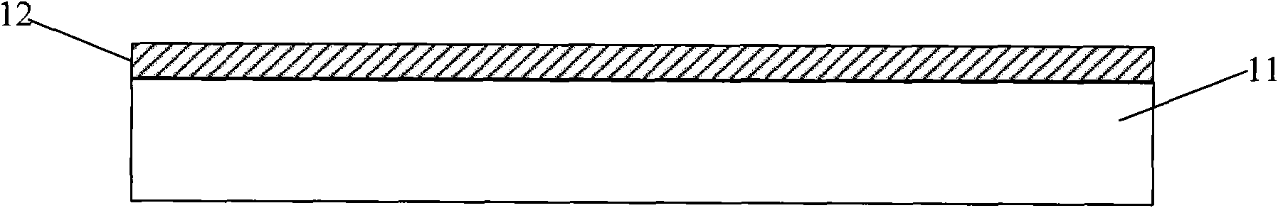
[0088] Firstly, the wafer is cleaned, and those skilled in the art can refer to the prior art to select suitable known means for cleaning. refer to Figure 1a , step S 11 , implant P-type ions, such as boron ions, into the surface of the N-type substrate 11 wafer by means of ion implantation, so as to form a P-type doped layer 12 . Preferably, the P-type doped layer is formed by implanting boron ions with an energy of 5keV and a concentration of 5E14-1E16, and the sheet resistance of the P-type doped layer is 40-200Ω / m 2 . The P-type ions implanted by ion implantation are annealed, the annealing temperature is higher than 900°C, and the annealing time is longer than 30 seconds, so as to activate the doping impurities. In addition, those skilled in the art can also choose other annealing methods according to actual needs. te...

Embodiment 2

[0105] refer to Figures 2a-2g , to introduce in detail the preparation method of the solar wafer described in Embodiment 2 of the present invention.

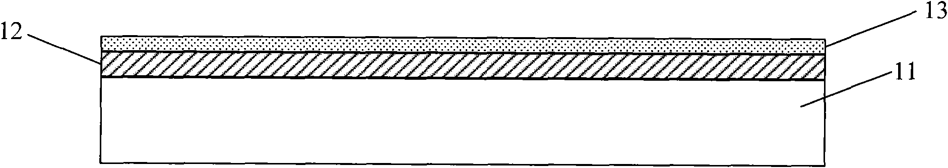
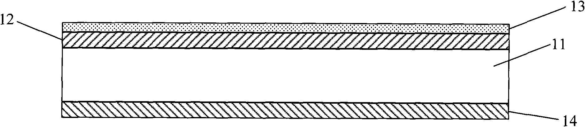
[0106] Firstly, the wafer is cleaned, and those skilled in the art can refer to the prior art to select suitable known means for cleaning. refer to Figure 2a , step S 21 1. Implanting P-type ions, such as boron ions, on the surface of the N-type substrate 21 wafer by ion implantation to form the P-type doped layer 22. Preferably, boron with an implantation energy of 5keV and a concentration of 5E14-1E16 can be used The ions form a P-type doped layer, and the sheet resistance of the P-type doped layer is 40-200Ω / m 2 .

[0107] refer to Figure 2b , step S 22 , forming an N+ type doped layer 23 on the back side of the N-type substrate 21 wafer, wherein phosphorus ions or arsenic ions with an energy of 30keV are implanted by ion implantation to form the N+ type doped layer, those skilled in the art can Select other ion impla...

Embodiment 3

[0121] Embodiment 3 The principle of the method for preparing a solar wafer is basically the same as that of Embodiment 2, the difference is that, with the following steps S 31 Replace step S in the second embodiment 21 : Implanting P-type ions on the surface of the N-type base wafer by means of ion implantation, and annealing the P-type ions, the annealing temperature is higher than 900°C, and the annealing time is longer than 30 seconds, to form a P-type doped layer, In addition, those skilled in the art can also select other annealing temperatures and times according to actual needs.

[0122] The structure of the solar wafer prepared in Example 3 is basically the same as in Example 2, except that the P-type doped layer on the surface of the N-type substrate is formed by annealing the P-type ions implanted by ion implantation. , wherein the annealing temperature is higher than 900°C and the annealing time is longer than 30 seconds.


PUM


Abstract

The invention discloses a solar wafer, which comprises an N-type substrate, a P-type mingling layer arranged on the surface of the N-type substrate, an N+-type mingling layer arranged on the back face of the N-type substrate, a first passivation layer arranged on the surface of the P-type mingling layer, a second passivation layer arranged on the surface of the first passivation layer, surface electrodes arranged on the second passivation layer and back face electrodes arranged on the N+-type mingling layer. The P-type mingling layer is formed by conducting annealing treatment on P-type ions injected in ion injection mode, annealing temperature is higher than 900 DEG C, and annealing time is more than 30 seconds. A preparation method of the solar wafer is further disclosed. The ion injection method is adopted to prepare the solar wafer so that dose, mingling depth and uniformity of mingled ions can be effectively and accurately controlled. Ideal square resistors can be obtained, and actually obtained solar conversion efficiency of products is higher and closer to laboratorial theoretical design value.

Description

technical field [0001] The invention relates to a solar wafer and a preparation method thereof, in particular to a solar wafer based on an N-type solar wafer and a preparation method thereof. Background technique [0002] New energy is one of the five most decisive technological fields in the world economic development in the 21st century. Solar energy is a clean, efficient and inexhaustible new energy source. In the new century, the governments of various countries regard the utilization of solar energy resources as an important content of the national sustainable development strategy. Photovoltaic power generation has the advantages of safety, reliability, no noise, no pollution, less constraints, low failure rate, and easy maintenance. In recent years, with the rapid development of international photovoltaic power generation, the supply of solar chips is in short supply, so improving the photoelectric conversion efficiency of solar chips and the production capacity of s...

Claims


Application Information

Patent Timeline
Patent Type & Authority Patents(China)
IPC IPC(8): H01L31/0352H01L31/18
CPCY02P70/50
Inventor 陈炯
Owner KINGSTONE SEMICONDUCTOR LIMITED COMPANY
Why Eureka
Try Eureka