

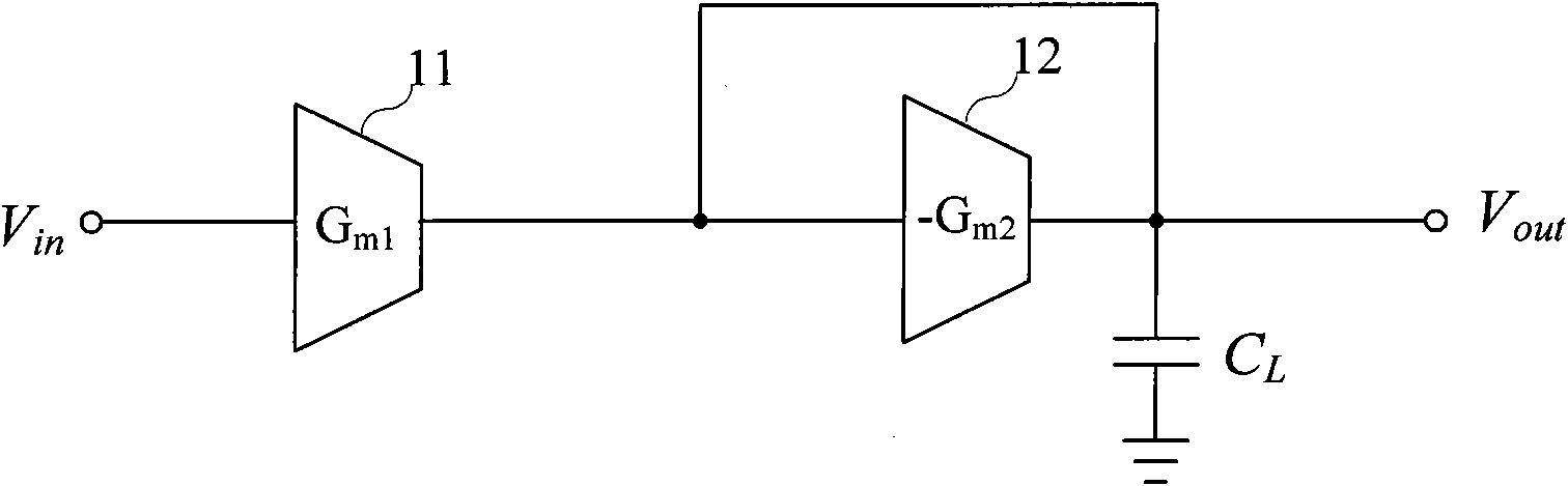
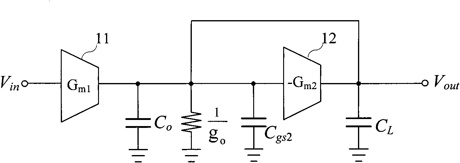
Wide band amplifier with frequency compensation
A frequency compensation and amplifier technology, applied in the field of wireless radio frequency communication, can solve the problems of difficulty in adjusting the output level of the output end of the broadband amplifier, the bandwidth is not easy to be made very high, and the power consumption is increased, so as to save power consumption, solve the gain and Output level, effect of reducing parasitic capacitance
- Summary
- Abstract
- Description
- Claims
- Application Information
AI Technical Summary
Problems solved by technology
Method used
Image

Examples
no. 1 example
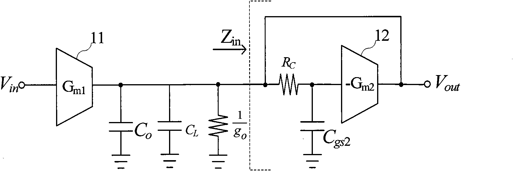
[0070] Figure 5a An implementation form of a broadband amplifier circuit in which the frequency compensation resistor is an active resistive element is given. The first transconductance amplifier module 51 adopts a source-level negative feedback transconductance structure to improve linearity and have a good suppression effect on common-mode signals. The second transconductance module 52 is an active load module, which adopts a pseudo-differential transconductance equivalent output resistance structure to improve the linearity of the load resistance, and at the same time allow the output common mode level to be directly coupled with the input stage of the subsequent circuit.
[0071] The first transconductance amplifier module 51 is composed of an input stage, a bias circuit, a tail current source, and a load current source. MOS tubes M5 and M6 form the tail current source; MOS tubes M1 and M2 form the differential input stage; MOS tubes M3 and M4 form the load current sourc...
Embodiment
[0074] Figure 5b Another implementation form of a broadband amplifier circuit in which the compensation resistor is a channel mask resistor is given. Amplifier circuit implementations in the form of Figure 5a The implementation form of the amplifier circuit is basically the same, and the two frequency compensation resistors R C+ and R C- It is a channel mask resistor, the process is simpler to realize, and the resistance value of the resistance element is adjusted by design during realization.
no. 3 example
[0076] The electrical schematic diagram of another embodiment of the broadband amplifier circuit using the frequency compensation technology proposed by the present invention is as follows Image 6 as shown, Image 6 A third embodiment of another implementation form of a broadband amplifier circuit with a different structure is given. The first transconductance amplifier module 61 adopts a classic fully differential transconductance amplifier structure with a tail current source, which saves power consumption and has a good suppression effect on common-mode signals. The second transconductance module 62 is an active load module, which adopts the same fully differential transconductance amplifier structure with a tail current source as the first transconductance amplifier module, which is equivalent to a load at the output end and saves power consumption. When the circuit with this structure is used, a common-mode feedback circuit (CMFB) needs to be used to stabilize the commo...
PUM
 Abstract
Description
Claims
Application Information