Method for manufacturing multilayer circuit board

A technology of multi-layer circuit board and manufacturing method, which is applied in the field of circuit board manufacturing, and can solve the problems of reducing production efficiency, increasing production precision requirements, and slow speed

Active Publication Date: 2012-03-21
AVARY HLDG (SHENZHEN) CO LTD +1
View PDF3 Cites 13 Cited by
  • Summary
  • Abstract
  • Description
  • Claims
  • Application Information

AI Technical Summary

Problems solved by technology

This makes the manufacturing process more complicated, increases the manufacturing precision requirements, and reduces the manufacturing efficiency.
In addition, in the prior art, only the mechanical drilling process or the laser drilling proc...

Method used


Image

  • Method for manufacturing multilayer circuit board
  • Method for manufacturing multilayer circuit board
  • Method for manufacturing multilayer circuit board

Examples


Embodiment Construction

[0051] The manufacturing method of the multilayer circuit board provided by this technical solution will be further described in detail below in conjunction with a number of drawings and implementations.

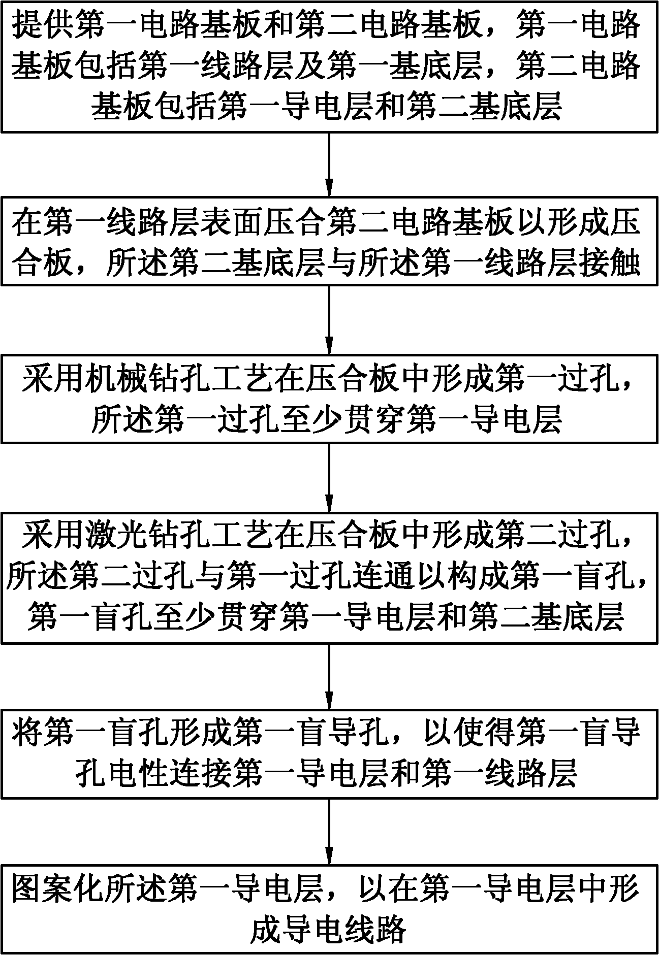
[0052] See figure 1 , The embodiment of the technical solution provides a manufacturing method of a multilayer circuit board, including the steps:

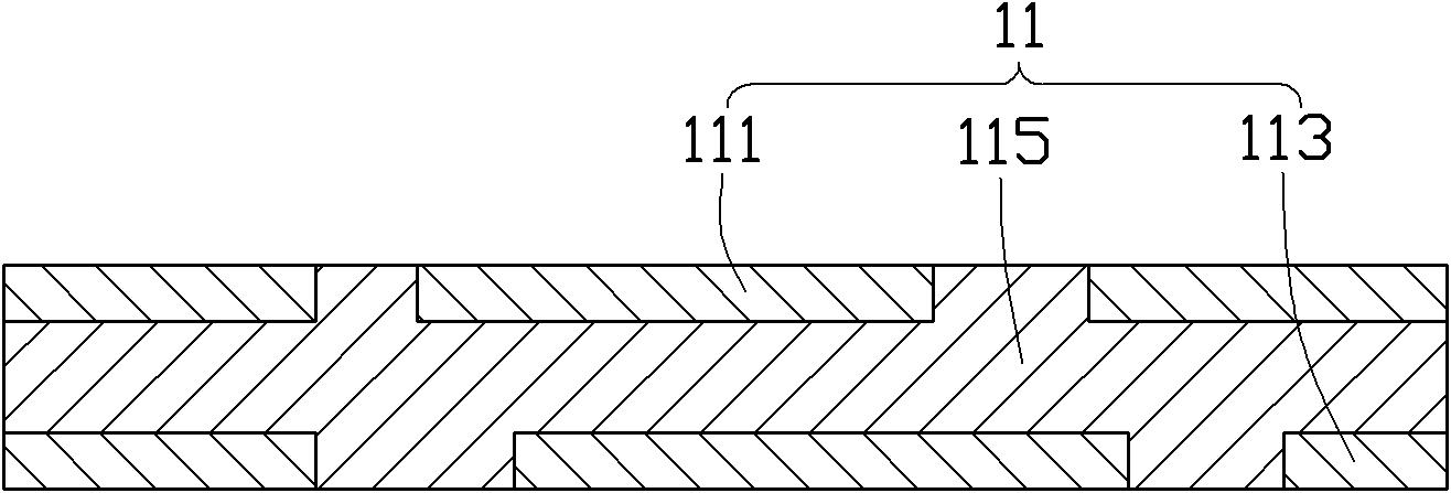
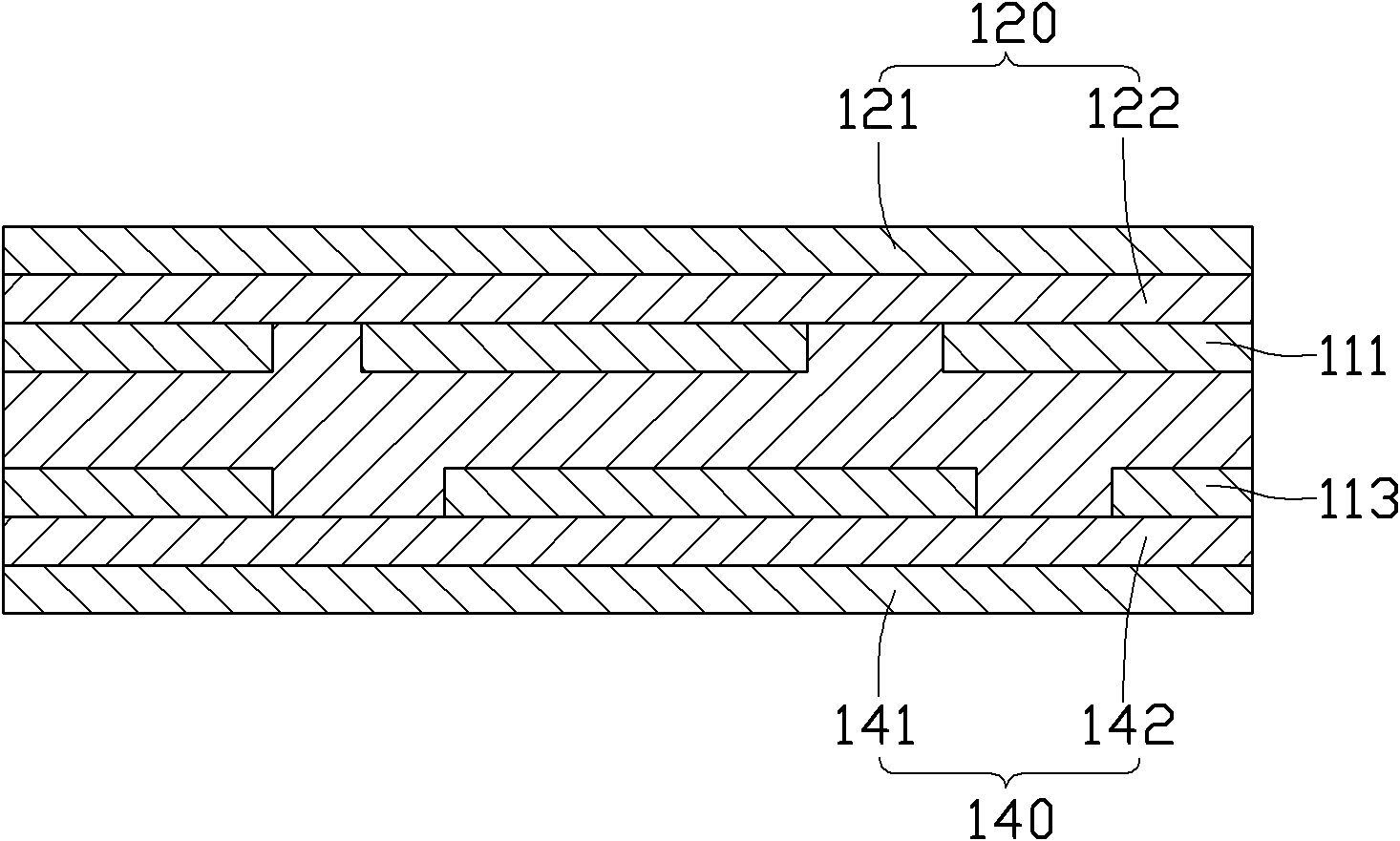
[0053] The first step, see figure 2 , Provide a first circuit substrate 11. The first circuit substrate 11 may be a single-layer board, a double-layer board or a multi-layer board. In this embodiment, the first circuit substrate 11 is a double-sided board for illustration. The first circuit substrate 11 includes a first circuit layer 111, a second circuit layer 113, and a first base layer 115 stacked in sequence.

[0054] The first circuit layer 111 and the second circuit layer 113 are located on both sides of the first base layer 115. The material of the first circuit layer 111 and the second circuit layer 113 can be one or an all...


PUM


Abstract

The invention provides a method for manufacturing a multilayer circuit board, which comprises the following steps of: providing a first circuit substrate and a second circuit substrate, wherein the first circuit substrate comprises a first circuit layer and a first substrate layer, and the second circuit substrate comprises a first conductive layer and a second substrate layer; laminating the second circuit substrate on the surface of the first circuit layer so as to form a laminated board, wherein the second substrate layer is in contact with the first circuit layer; forming a first via holein the laminated board by adopting a mechanical drilling process, wherein the first via hole at least penetrates through the first conductive layer; forming a second via hole in the laminated board by adopting a laser drilling process, wherein the second via hole is communicated with the first via hole so as to compose a first blind hole, and the first blind hole at least penetrates through the first conductive layer and the second substrate layer; making a first blind guide hole from the first blind hole, so that the first blind guide hole is electrically connected with the first conductive layer and the first circuit layer; and patterning the first conductive layer so as to form a conductive circuit in the first conductive layer.

Description

Technical field [0001] The invention relates to a circuit board manufacturing technology, in particular to a manufacturing method of a multilayer circuit board. Background technique [0002] In the information, communication and consumer electronics industries, circuit boards are an indispensable basic component of all electronic products. With the development of electronic products in the direction of miniaturization and high-speed, circuit boards have also developed from single-sided circuit boards to double-sided circuit boards and multilayer circuit boards. Multi-layer circuit boards are widely used due to their larger wiring area and higher assembly density. Please refer to Takahashi, A. et al. in 1992 published in IEEE Trans. on Components, Packaging, and Manufacturing Technology "High density multilayer printed circuit board for HITACM~880". [0003] The multi-layer circuit board has multiple conductive layers, and the multiple conductive layers realize signal connection t...

Claims


Application Information

Patent Timeline
IPC IPC(8): H05K3/46
Inventor 刘瑞武
Owner AVARY HLDG (SHENZHEN) CO LTD
Why Eureka
Try Eureka