Multi-micropacket parallel processing structure

A parallel processing, micro-packet technology, used in error prevention/detection using return channels, digital transmission systems, electrical components, etc. Problems such as the processing speed of the point controller chip and the increase in data transmission delay

Inactive Publication Date: 2012-03-28
NAT UNIV OF DEFENSE TECH
View PDF5 Cites 16 Cited by
  • Summary
  • Abstract
  • Description
  • Claims
  • Application Information

AI Technical Summary

Problems solved by technology

For example, according to the evaluation of ASIC chip manufacturer's process library and RAM IP (Intellectural Property, intellectual property core) library, under the 90nm process, standard units such as registers can work at about 1GHz, but the maximum operating frequency of IP such as RAM is 500MHz, and With the increase of RAM capacity, the working frequency shows a downward tre...

Method used


Image

  • Multi-micropacket parallel processing structure
  • Multi-micropacket parallel processing structure
  • Multi-micropacket parallel processing structure

Examples


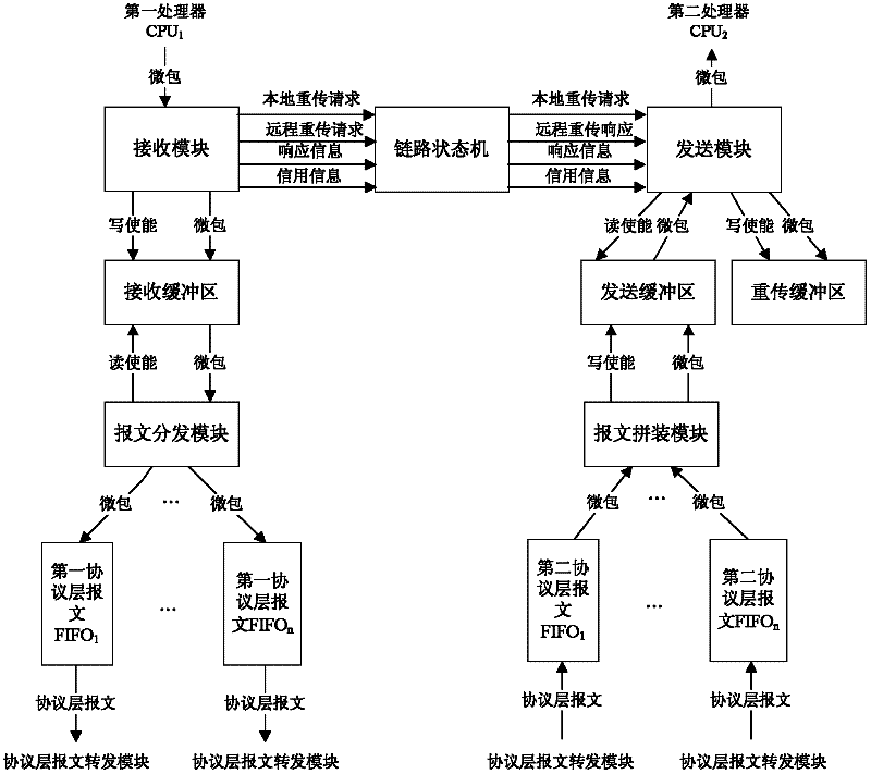
Embodiment Construction

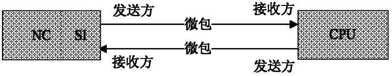
[0045] figure 1 It is a schematic diagram of the direct connection communication between the node control chip NC and the processor CPU in the background technology.

[0046] The node control chip is directly connected to the processor, and the processor interface access control component SI in the node control chip is responsible for reliable data transmission between the processor and the node control chip, and performs flow control and error detection / correction based on the credit mechanism . The SI includes a receiving module and a sending module. The sending module is responsible for sending messages to the processor, and the receiving module receives messages from the processor. Therefore, message transmission is divided into sender and receiver, and the receiver and sender belong to different ports: when SI sends a message to the processor, the sender is SI, and the receiver is the processor; when SI receives a message from the processor In the case of a message, the...


PUM


Abstract

The invention discloses a multi-micropacket parallel processing structure, which aims to solve the problem that in a single-micropacket processing structure, the bandwidth of a physical layer and a link layer is not matched, so that the speed of the processing of the chip of a node controller to the communication among processors is reduced. The multi-micropacket parallel processing structure comprises an interface conversion module, a receiving module, a receiving buffer area, a message distribution module, a first protocol layer message FIFO (First In First Out), a second protocol layer message FIFO, a link state machine, a message assembly module, a send buffer area, a retransmission buffer area and a sending module, wherein the interface conversion module works under a physical layer clock domain, other modules work under a link layer clock domain, the interface conversion module comprises asynchronous receiving FIFO and asynchronous transmission FIFO, and data paths in the receiving module and the sending module are multi-path parallel data paths aiming at multi micropackets, and can process the multi micropackets in parallel. According to the invention, the bandwidth of the physical layer/the link layer is matched, so that the speed of the processing of the chip of the node controller to the communication among the processors is improved.

Description

technical field [0001] The invention relates to a flit processing structure in a processor interface access part in a node control chip. Background technique [0002] In the computer structure, the node control chip (Node Controller, NC), that is, the north bridge chip, is the core chip second only to the processor. [0003] Node control chip design techniques are developed in tandem with processor architecture and interface technology evolutions to match processor capabilities and requirements. Processor interface technology is gradually transitioning from front side bus FSB (Front Side Bus) to high-speed direct connection interface technology, such as AMD's HT (HyperTransport) interface and Intel's QPI (Quick Path Interconnect) interface. With the development of the processor direct connection interface technology, the multi-processor direct connection architecture has become the mainstream structure for building servers or mainframes. Note that the scale of multi-proces...

Claims


Application Information

Patent Timeline
IPC IPC(8): H04L1/18H04L1/00H04L12/56
Inventor 庞征斌徐炜遐张峻夏军陆平静童元满常俊胜王绍刚齐星云张建民徐金波董德尊
Owner NAT UNIV OF DEFENSE TECH
Why Eureka
Try Eureka