Anti-dazzle Thin Film And Liquid Crystal Display Device

A liquid crystal display device and film technology, applied in optics, instruments, nonlinear optics, etc., can solve problems such as glare and insufficient precision of concave and convex shapes, achieve good contrast and wide viewing angle characteristics, and prevent visual recognition Reduced, excellent anti-glare effect

Active Publication Date: 2012-04-04
SUMITOMO CHEM CO LTD
View PDF16 Cites 19 Cited by
  • Summary
  • Abstract
  • Description
  • Claims
  • Application Information

AI Technical Summary

Problems solved by technology

[0019] However, since the anti-glare film described in JP-A-2008-209861 is produced using an embossing die in which concavo-convex shapes are formed by sandblasting, the accuracy of the concavo-convex shapes is not sufficient, and in particular, it may have a period of 50 μm or more. The relatively large concave-convex shape has the problem of "flicker"

Method used


Image

  • Anti-dazzle Thin Film And Liquid Crystal Display Device
  • Anti-dazzle Thin Film And Liquid Crystal Display Device
  • Anti-dazzle Thin Film And Liquid Crystal Display Device

Examples


Embodiment 1

[0255] (Preparation of molds for anti-glare film production)

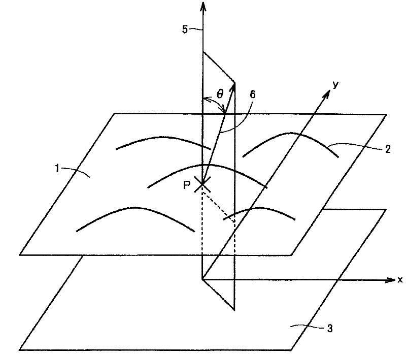
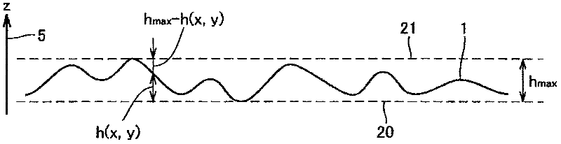
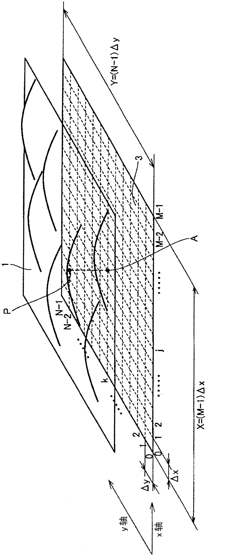
[0256] The roll which gave the ballard copper plating to the surface of the aluminum roll (A5056 of JIS) of diameter 200mm was prepared. Ballard copper plating consists of copper plating layer / thin silver plating layer / surface copper plating layer, and the overall thickness of the plating layer is set to 200 μm. The copper-plated surface is mirror-polished, a photosensitive resin is coated on the polished copper-plated surface, and dried to form a photosensitive resin film. Next, the following pattern is exposed and developed on the photosensitive resin film by laser light, and the pattern is Figure 16 The pattern shown (by removing 0.035 μm from the pattern with random brightness distribution -1 Below the low spatial frequency components and 0.15μm -1 The band-pass filter of the above high spatial frequency components) is repeated and juxtaposed. Laser exposure and development were performed with Laser Stream...

Embodiment 2

[0265] A mold B was produced in the same manner as in Example 1 except that the etching amount of the second etching process was set to 8 μm, and an antiglare film B was produced in the same manner as in Example 1 except that the mold B was used.

Embodiment 3

[0267] A mold C was produced in the same manner as in Example 1 except that the etching amount of the second etching process was set to 10 μm, and an antiglare film C was produced in the same manner as in Example 1 except that the mold C was used.


PUM

PropertyMeasurementUnit
mean roughnessaaaaaaaaaa
thicknessaaaaaaaaaa
hazeaaaaaaaaaa

Abstract

The invention provides an anti-dazzle thin film and a liquid crystal display device. The anti-dazzle thin film comprises a transparent supporting body and an anti-dazzle layer, wherein the anti-dazzle layer, formed upon the transparent supporting body, comprises a minuteness concave-convex surface having minor concavo and convex at the side opposite to the transparent supporting body. The anti-dazzle thin film is characterized in that: the internal haze is below 1% while the surface haze is between 0.4% and 10%; the imagine plane, incoming from the main normal direction of the mean surface of the minuteness concave-convex surface and containing the points having highest level, is parallel to the mean surface of the concave-convex surface, that is, the wavelength ejected by the highest level surface is 550nm; the plural amplitude of the highest level surface can be calculated via the level of the minuteness concave-convex surface and the refractive index of the anti-dazzle layer; and when the one-dimensional power spectrum of the plural amplitude is employed as a graph to indicate the intensity of the spatial frequency, there are two break points within the spatial frequency range of 0.032 micron-1 to 0.064 micron-1.

Description

technical field [0001] The present invention relates to an anti-glare (anti-glare) film excellent in anti-glare properties and a liquid crystal display device having the anti-glare film. Background technique [0002] [Anti-glare film] [0003] For image display devices such as liquid crystal displays and plasma display panels, Braun tube (cathode ray tube: CRT) displays, organic electroluminescent (EL) displays, when external light is projected on the display surface, visual recognition Sexuality will be significantly impaired. In order to prevent the reflection of this kind of external light, in TVs and personal computers that value image quality, video cameras and digital cameras used outdoors where the external light is strong, and mobile phones that use reflected light for display, image An anti-glare film is used on the surface of the display device to prevent reflection of external light. [0004] As such an anti-glare film, for example, JP-A-2006-53371 describes an...

Claims


Application Information

Patent Timeline
Patent Type & Authority Applications(China)
IPC IPC(8): G02B5/02G02B1/10G02F1/1335
CPCB29C59/04B29D11/0074B29D11/00788G02B5/0221G02B5/0257G02B5/0278G02F1/1396
Inventor 古谷勉藤井贵志神野亨
Owner SUMITOMO CHEM CO LTD
Why Eureka
Try Eureka