Fast recovery diode (FRD) device structure and manufacturing method thereof

A technology of device structure and manufacturing method, applied in semiconductor/solid-state device manufacturing, semiconductor devices, electrical components, etc., can solve the problems of increasing the forward conduction voltage drop of holes, unfavorable process production, expensive equipment, etc., to improve the on-state The effect of pressure drop, improving production efficiency, and improving emission efficiency

Active Publication Date: 2012-05-02
SHANGHAI INTEGRATED CIRCUIT RES & DEV CENT
View PDF6 Cites 2 Cited by
  • Summary
  • Abstract
  • Description
  • Claims
  • Application Information

AI Technical Summary

Problems solved by technology

However, the method of reducing the carrier lifetime to improve the reverse recovery characteristics and reduce the hole injection efficiency will increase the pressure drop of the forward conduction, and the method of injecting high-energy hydrogen ions, helium ions and other local recombination centers uses very expensive equipment. Not conducive to process production

Method used


Image

  • Fast recovery diode (FRD) device structure and manufacturing method thereof
  • Fast recovery diode (FRD) device structure and manufacturing method thereof
  • Fast recovery diode (FRD) device structure and manufacturing method thereof

Examples


Embodiment Construction

[0030] In order to make the content of the present invention clearer and easier to understand, the content of the present invention will be further described below in conjunction with the accompanying drawings. Of course, the present invention is not limited to this specific embodiment, and general replacements known to those skilled in the art are also covered within the protection scope of the present invention.

[0031] Secondly, the present invention is described in detail by means of schematic diagrams. When describing the examples of the present invention in detail, for the convenience of explanation, the schematic diagrams are not partially enlarged according to the general scale, which should not be used as a limitation of the present invention.

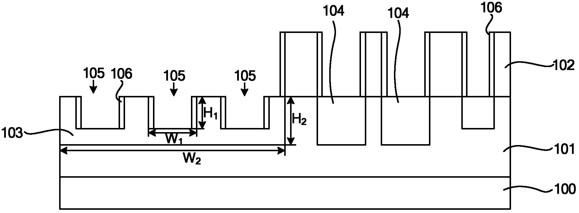
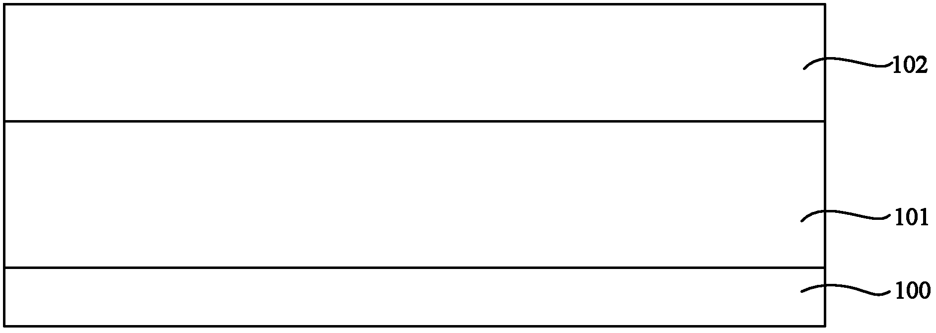
[0032] The invention provides a FRD device structure, figure 1 It is the FRD device structure in an embodiment, such as figure 1 As shown, the FRD device structure includes: an N-type heavily doped layer 100; an N-type doped...


PUM


Abstract

The invention provides a fast recovery diode (FRD) device structure and a manufacturing method thereof. An insulation layer is formed on the side wall of a trench of the FRD device structure, and the insulation layer is combined with the surface of a P-type doped region to form a combining center, so that a combining route from the P-type doped region to the insulation layer is formed, and the reverse recovery characteristic of the device is improved effectively; furthermore, due to the presence of the insulation layer on the side wall of the trench, partial combined current carriers which reach the upper surface of the P-type doped region from the P-type doped region through the combining route are shielded by the insulation layer and combined on the surface of the insulation layer, so that the emission efficiency is improved and the state voltage drop is reduced; moreover, the doping concentration at the bottom of the trench in the P-type doped region is controlled, so that the diffusion length of the current carriers is prevented from being dramatically reduced, the scattering of the current carriers and an auger combining effect are avoided, the emission efficiency of the bottom region of the trench in the P-type doped region is improved, the rising of the state voltage drop of the trench caused by doping reduction is compensated, and the forward voltage drop is improved.

Description

technical field [0001] The invention relates to a device structure and a manufacturing method in the field of integrated circuit manufacturing, in particular to an FRD structure and a manufacturing method thereof. Background technique [0002] With the continuous reduction of oil and coal reserves, and the continuous increase of human energy consumption, energy conservation has become the consensus of human beings in the 21st century. The U.S. Department of Energy estimates that two-thirds of electricity is used to drive motors. The use of IGBT and its matching FRD and other power devices can make the motor drive energy-saving by 20% to 30%. It can be expected that power devices will grow rapidly in the future. [0003] For FRD (Fast recovery diode, fast recovery diode) power devices, its reverse recovery characteristics and forward conduction voltage drop are very important. High forward conduction voltage drop means low energy conversion efficiency, and poor reverse reco...

Claims


Application Information

Patent Timeline
Patent Type & Authority Applications(China)
IPC IPC(8): H01L29/861H01L29/06H01L21/329
Inventor 孙德明
Owner SHANGHAI INTEGRATED CIRCUIT RES & DEV CENT
Why Eureka
Try Eureka