Optical memory device and method of recording/reproducing information by using the same

A storage device, optical technology, applied in the fields of recording/reproducing by optical methods, digital memory information, nanotechnology for information processing, etc., can solve the problems of optical storage and other problems

Inactive Publication Date: 2012-05-02
SAMSUNG ELECTRONICS CO LTD
View PDF3 Cites 2 Cited by
  • Summary
  • Abstract
  • Description
  • Claims
  • Application Information

AI Technical Summary

Problems solved by technology

Various types of optical memory devices have been proposed, however, no optical memory having a structure of recording / reproducing properties that can replace conventional memories has been proposed

Method used


Image

  • Optical memory device and method of recording/reproducing information by using the same
  • Optical memory device and method of recording/reproducing information by using the same
  • Optical memory device and method of recording/reproducing information by using the same

Examples


Embodiment Construction

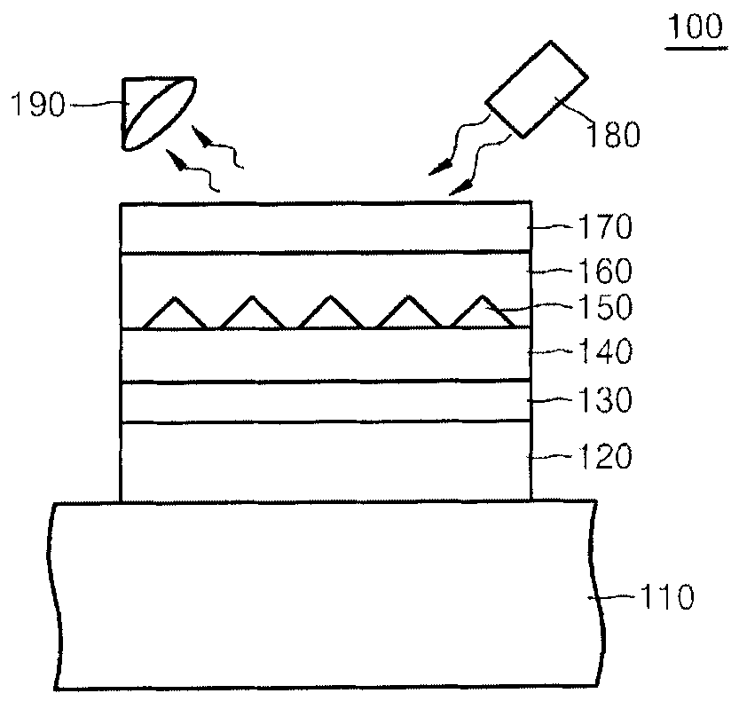
[0047] The present invention will now be described more fully with reference to the accompanying drawings, in which exemplary embodiments of the invention are shown. However, this invention may be embodied in many different forms and should not be construed as limited to the embodiments set forth herein; rather, these embodiments are provided so that this disclosure will be thorough and complete, and will incorporate the present invention The concepts are fully conveyed to those of ordinary skill in the art. In the drawings, the thicknesses of layers and regions are exaggerated for clarity. In the drawings, the same reference numerals denote the same elements, and thus their detailed descriptions will be omitted.

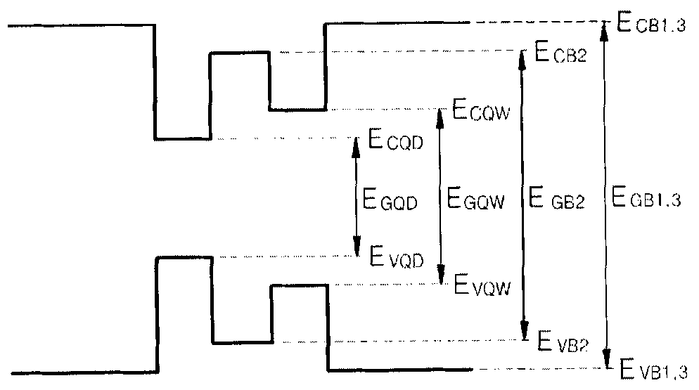
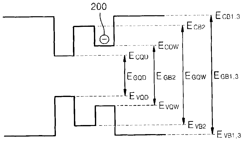
[0048] figure 1 is a cross-sectional view of an optical storage device 100 according to an embodiment of the present invention, figure 2 and image 3 are shown respectively figure 1 A diagram of the energy bands of the optical storage device 100 in a non-recor...


PUM

PropertyMeasurementUnit
thicknessaaaaaaaaaa

Abstract

Provided are optical memory device and a method of recording/reproducing information by using the optical memory device. The optical memory device includes a substrate; a first barrier layer formed on the substrate; a quantum well layer; a second barrier layer; a quantum dot layer; and a third barrier layer. The quantum well layer has an energy band gap which is wider than that of the quantum dot layer, and the second barrier layer has an energy band gap which is wider than that of the quantum well layer, so that electrons in excitons which are generated in the quantum dot layer by light of a certain wavelength are captured by the quantum well layer to record information, and then, recorded information may be erased or reproduced by irradiating light of a certain wavelength to the optical memory device.

Description

technical field [0001] The present invention relates to an optical storage device and a method for recording / reproducing information using the optical storage device, and more particularly, to an apparatus and method for recording / reproducing information using the optical properties of quantum dots. Background technique [0002] Due to the rapid development of information and communication technology, the transmission capacity or information volume of the network has greatly increased. Optical fibers are used to achieve high-speed and large-capacity transmission on the network, however, in order to process information, optical signals are converted into electrical signals at nodes of the network. [0003] Since optical signals are converted into electrical signals, the communication rate on the network is limited. Therefore, there is a need for an optical information processing technology that can process information without converting an optical signal into an electrical s...

Claims


Application Information

Patent Timeline
Patent Type & Authority Applications(China)
IPC IPC(8): G11B7/00G11B9/00G11C13/06
CPCB82Y10/00G11B9/149G11B11/002G11C13/047G11C13/04G11B7/00G11B9/00G11C13/06H01L27/14601H01L27/14603H01L27/14609H01L27/14647H01L33/06
Inventor 裴在喆金朱镐李镇京
Owner SAMSUNG ELECTRONICS CO LTD
Why Eureka
Try Eureka