System and method for wafer back-grinding control

A technology of back grinding and control system, which is applied in semiconductor/solid-state device manufacturing, grinding automatic control device, semiconductor/solid-state device testing/measurement, etc. It can solve the problem of reducing the size of semiconductors and achieve the effect of reducing process defects

Active Publication Date: 2012-05-09
TAIWAN SEMICON MFG CO LTD
View PDF4 Cites 7 Cited by
  • Summary
  • Abstract
  • Description
  • Claims
  • Application Information

AI Technical Summary

Problems solved by technology

[0002] The continuing trend of shrinking semiconductor dimensions faces multiple challenges

Method used


Image

  • System and method for wafer back-grinding control
  • System and method for wafer back-grinding control
  • System and method for wafer back-grinding control

Examples


Embodiment Construction

[0017] In the following description, "an embodiment" in different paragraphs does not necessarily refer to a single embodiment, and the structure can be implemented in at least one embodiment. In general, the same reference numerals are used to designate similar structures, but this does not mean that elements with the same reference numerals in each embodiment have the same structure. In addition, the structures in the illustrations are not completely drawn to scale, so the dimensions in the illustrations are not intended to limit the system described below.

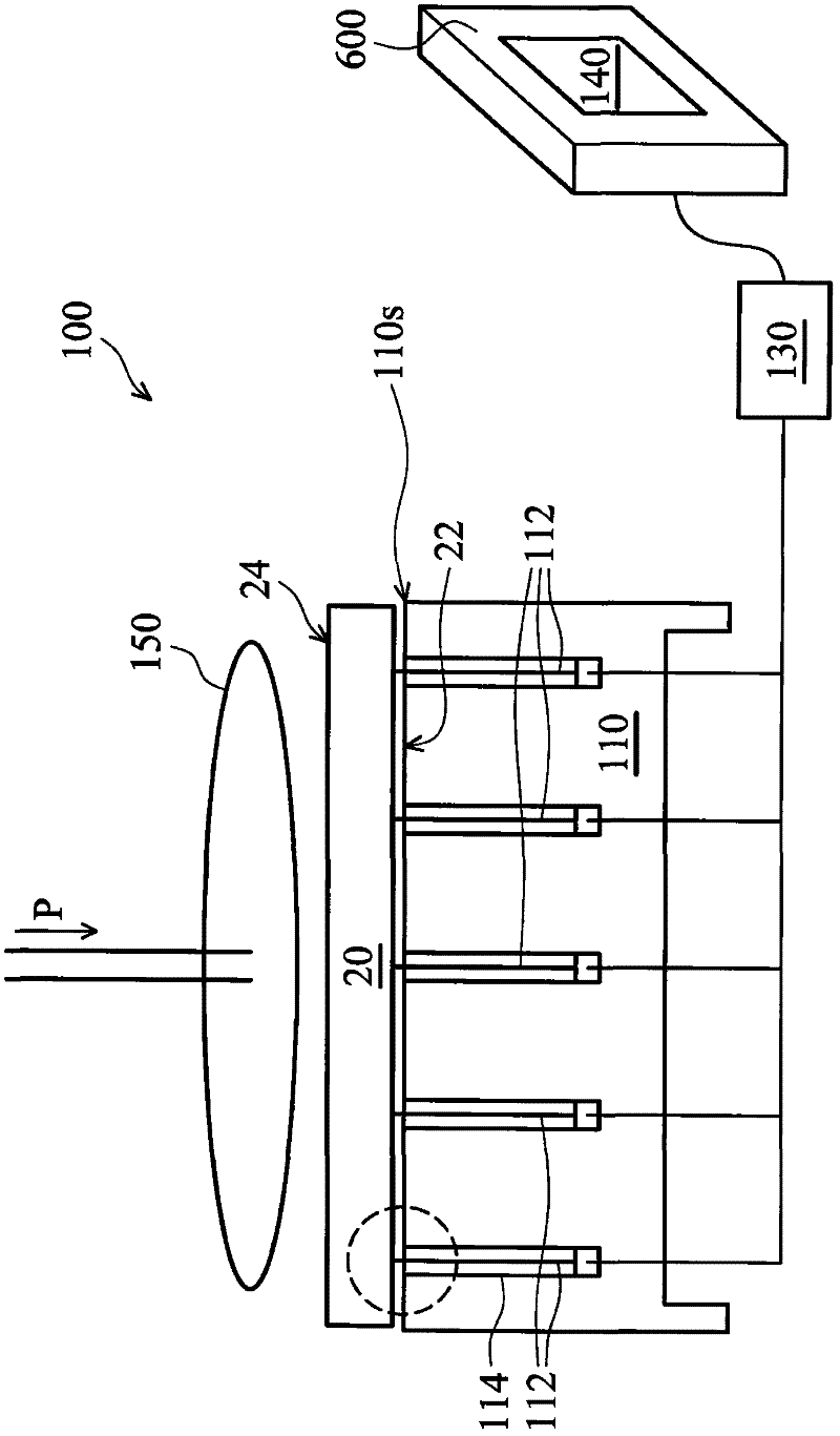
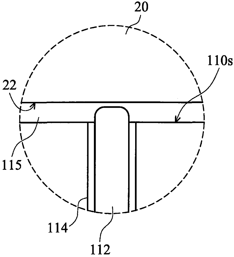
[0018] In the following description and accompanying drawings, at least one semiconductor wafer 20 (see Figure 1A ) are ground to remove excess substrate. Before the semiconductor wafer 20 is placed on the back grinding device, a grinding tape (not shown) is attached to the front side 22 of the semiconductor wafer by a device (not shown or labeled). The abrasive tape on the front side 22 of the semiconductor wafer pro...


PUM


Abstract

In a system or method for controlling wafer back-grinding, a chuck table has a surface for supporting a semiconductor wafer during a back-grinding process, one or more holes in the surface, and one or more sensors disposed in the one or more holes for monitoring a parameter during back-grinding. A computer-implemented process control tool is coupled to receive one or mote outputs from the one or more sensors and control the back-grinding process based on the received one or more outputs. The system and method for wafer back-grinding control can effectively reduce process defects and enable the thickness of the semiconductor wafer to be consistent in the process of back-grinding.

Description

technical field [0001] The present invention relates to reducing process defects such as wafer breakage or warpage, and more particularly to achieving consistent thickness of semiconductor wafers during backgrinding processes. Background technique [0002] The continued trend to shrink the size of semiconductors faces multiple challenges. In the mass production process of integrated circuits, one of the methods to reduce the size is to use extremely thin semiconductor wafers. Some known inventors in the art employ back grinding to reduce the thickness of semiconductor wafers. In fact, the operation is to complete the front (or active surface) components of the semiconductor wafer first, and then remove the excess substrate from the back of the wafer. [0003] In the back grinding process, the wafer is first placed on the table, and then the excess substrate is removed with a grinding wheel. Some systems may have multiple separate grinding wheels, with one grinding wheel g...

Claims


Application Information

Patent Timeline
IPC IPC(8): B24B37/005H01L21/00H01L21/304H01L21/66
CPCB24B51/00H01L21/67265B24B49/16B24B7/228H01L21/304B24B41/061
Inventor 卢祯发李江浩陈威宇刘重希
Owner TAIWAN SEMICON MFG CO LTD
Why Eureka
Try Eureka