Check patentability & draft patents in minutes with Patsnap Eureka AI!

A kind of preparation method of memory unit

A memory unit and device technology, which is applied in semiconductor/solid-state device manufacturing, electrical components, circuits, etc., can solve problems such as hole accumulation and substrate current cannot be released, and achieve the effect of increasing writing speed and substrate current

Active Publication Date: 2016-08-10
SHANGHAI HUALI MICROELECTRONICS CORP
View PDF2 Cites 0 Cited by
  • Summary
  • Abstract
  • Description
  • Claims
  • Application Information

AI Technical Summary

Problems solved by technology

Due to the existence of the oxygen buried layer, the substrate current cannot be released, so that the holes accumulate in the floating

Method used


Image

  • A kind of preparation method of memory unit

Examples


preparation example Construction

[0014] The present invention provides a method for preparing a memory cell, which includes performing a ring-shaped implantation process on the memory cell, wherein the ring-shaped implantation process includes forward implantation and reverse implantation, wherein the ions implanted in the forward direction are of an inverse type to that of source and drain The ions implanted in reverse are of the same type as the source and drain ions, and the ions are implanted into the channel of the device.

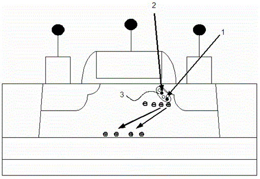
[0015] In the usual process, in order to suppress the short channel effect (Short Channel Effect) of the device, ring implantation is used to implant the ions of the opposite type to the source and drain into the device channel. Such as figure 1 As shown, taking an NMOS device as an example, the channel direction of the device in the middle figure is defined as the x direction, and the vertical direction of the silicon wafer surface in the figure is defined as the y direction. When ...


PUM


Abstract

The invention provides a method for preparing a memory cell, which includes performing a ring-shaped implantation process on the memory cell. The ring-shaped implantation process includes forward implantation and reverse implantation, wherein the number of gains and losses of the outermost layer of reverse implanted ions is the same as In contrast to forward implantation of ions, the ions are implanted into the device channel. In the method for preparing memory cells provided by the present invention, the reverse implantation method is added to the circular implantation process during the preparation of floating body effect memory cells, and the current carrying capacity is enhanced at the drain end while keeping the total implantation dose constant. The impact ionization rate between electrons and impurity scattering centers, thereby increasing the substrate current of the floating body effect memory cell, and improving the writing speed of the floating body effect memory cell.

Description

technical field [0001] The invention relates to the field of semiconductor preparation, in particular to a preparation method capable of improving the writing speed of a floating body DRAM. Background technique [0002] The development of embedded dynamic memory technology has made large-capacity DRAM very common in current system-on-chip (SOC). Large-capacity embedded dynamic memory (eDRAM) brings various benefits to SOCs, such as improved bandwidth and reduced power consumption, that can only be realized by using embedded technology. In addition to the transistor, each storage unit of the traditional embedded dynamic memory needs a deep trench capacitor structure. The deep trench of the capacitor makes the height of the storage unit much larger than its width, which makes the manufacturing process difficult. Its manufacturing process is very incompatible with CMOS VLSI process, which limits its application in embedded system-on-chip (SOC). [0003] Floating Body Cell (FB...

Claims


Application Information

Patent Timeline
Patent Type & Authority Patents(China)
IPC IPC(8): H01L21/265H01L21/8242H10B12/00
Inventor 俞柳江
Owner SHANGHAI HUALI MICROELECTRONICS CORP
Features
  • R&D
  • Intellectual Property
  • Life Sciences
  • Materials
  • Tech Scout
  • Unparalleled Data Quality
  • Higher Quality Content
  • 60% Fewer Hallucinations
Learn More